The ADP1196ACBZ-R7 is a high-side or low-side load switch designed for VIN operation between 0 V and 5.5 V with a VB_EN supply of 1.83 V to 5.5 V. The device contains an internal charge pump that operates from either VIN or VB_EN, whichever is higher, and an ultralow on resistance, N-channel MOSFET. This N-channel MOSFET supports more than 2 A of continuous current at VIN close to 0 V, and, with its ultralow on resistance, minimizes power loss. In addition, the on resistance is constant, independent of the VIN or VB_EN voltage. The low 26 μA quiescent current and ultralow shutdown current make the ADP1196ACBZ-R7 ideal for low power applications.
When the junction temperature exceeds 125°C, overtemperature protection circuitry is activated, thereby protecting the ADP1196ACBZ-R7 and downstream circuits from potential damage.
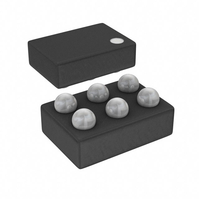
The ADP1196ACBZ-R7 occupies minimal printed circuit board (PCB) space, with an area of less than 1.5 mm2 and a height of 0.60 mm.
The ADP1196ACBZ-R7 is available in an ultrasmall 1.0 mm × 1.5 mm, 6-ball, 0.5 mm pitch WLCSP.
Feature
- Low RDSON of 10 mΩ in 6-ball WLCSP
- Wide input voltage range: 0 V to 5.5 V
- 3 A continuous operating current at 70°C
- Bias supply voltage range 1.83 V to 5.5 V
- Low 26 μA ground (quiescent) current, VIN ≤ 3.4 V
- Low 50 μA quiescent current,VIN = 5.5 V
- Overtemperature protection circuitry
- Low shutdown current: <3.5 μA
- Ultra-small 1.0 mm × 1.5 mm, 6-ball, 0.5 mm pitch WLCSP
Applications
- Communications and InfrastructureTEC Controller reverse polarity for Heating/CoolingFine Line Geometry Core Voltage In-rush current control
- Medical and Healthcare
- Instrumentation
(Picture: Pinout)

