HV816K6-G is a high voltage Electroluminescent (EL) lamp driver designed for driving a lamp capacitance of up to 150nF, or an area of approximately 42 square inches. It is comprised of a boost converter followed by an H-bridge. The boost converter produces a regulated output voltage, which is set at a nominal value of 180V using an internal reference voltage. The H-bridge is used to produce a differential output drive and the EL lamp will therefore see ±180V (360V peak-to-peak). The HV816K6-G has two internal oscillators, one for controlling the boost converter switching frequency and the other for controlling the H-bridge switching frequency. Having separate control of each switching frequency allows flexibility in the circuit design.The operating input supply voltage is 2.7 to 5.5V, but the Enable (EN) and Select (SEL) interface to the device will accept logic high levels down to 1.5V. The EN input is for turning the device ON and OFF. The SEL input is for external logic control of the H-bridge switching frequency, if required. The HV816K6-G boost converter stage uses a single inductor and a minimum number of external components. The input voltage to the inductor can be different from the input voltage to the HV816K6-G (split supply). The external inductor is connected either between the LX and VDD pins or, for split supply applications, between the LX pin and a higher voltage supply (shown as VIN in the Block Diagram). An external MOSFET has to be driven by the switch oscillator to generate a high voltage. The switching frequency for this MOSFET is set by an external resistor connected between the RSW-Osc pin and the supply pin VDD. During operation, the external switching MOSFET turns on and allows energy to be stored in the inductor; this energy is transferred into the capacitor CS when the MOSFET turns off. The voltage at the CS pin will increase with every switching cycle. Once the voltage at the CS pin reaches the desired regulation limit, nominally 180V, the external switching MOSFET is turned OFF to conserve power.The CS capacitor is connected between the CS pin and ground; the CS pin is internally connected to the H-bridge. Energy from the boost converter stage is stored in the capacitor before being transferred to the EL lamp. Depending on the EL lamp sizes, a 1.0nF to 15nF capacitor should be used for CS. The EL lamp switching frequency can be in the range of 100Hz to 1.0kHz. This frequency can be set by either an external logic signal at the SEL pin, with a frequency that is 4 times the desired EL lamp switching frequency, or by an external resistor connected between the REL-Osc and VDD pins. If external frequency is input to the device at the SEL pin, the REL-Osc pin should be connected to ground.The HV816K6-G has the provision to control the discharge rate of the output to minimize audible noise emitted by the EL lamp, which is connected between the VA and VB pins. An external resistor from the RSLEW-OUT pin to ground controls the VA, VB output discharge rate. EL lamp dimming can be accomplished by changing the input voltage to the VREG pin. The VREG pin allows an external voltage source to control the VCS amplitude. The VCS voltage is approximately 143 times the voltage at the VREG pin.
High Voltage Electroluminescent Backlight Driver ICs High Voltage Electroluminescent Backlight Driver ICs
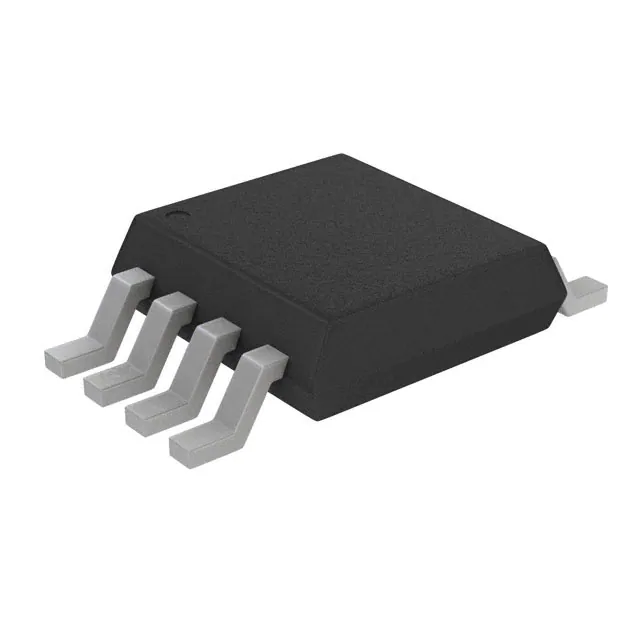
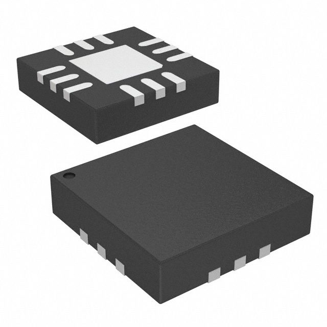
Features360VPP output voltage for high brightness Large output load capability to 5.5V operating supply voltage Single lithium ion cell compatible Adjustable output regulation for dimming External switching MOSFET Low audible noise Output discharge slew rate control 1.5V logic Dedicated Enable pin Two EL frequency controls Independent lamp and converter frequency setting Split supply capability Available in 4x4 QFN and 16-Lead SOW packages
logic high levels down to 1.5V. The EN input is for turning the device ON and OFF. The SEL input is for external logic control of the H-bridge switching frequency, if required. The HV816K6-G boost converter stage uses a single inductor and a minimum number of external components. The input voltage to the inductor can be different from the input voltage to the HV816K6-G (split supply). The external inductor is connected either between the LX and VDD pins or, for split supply applications, between the LX pin and a higher voltage supply (shown as VIN in the Block Diagram). An external MOSFET has to be driven by the switch oscillator to generate a high voltage. The switching frequency for this MOSFET is set by an external resistor connected between the RSW-Osc pin and the supply pin VDD. During operation, the external switching MOSFET turns on and allows energy to be stored in the inductor; this energy is transferred into the capacitor CS when the MOSFET turns off. The voltage at CS will increase with every switching cycle. Once the voltage at CS reaches the desired regulation limit, nominally 180V, the external switching MOSFET is turned OFF to conserve power. The CS capacitor is connected between the CS pin and ground; the CS pin is internally connected to the H-bridge. Energy from the boost converter stage is stored in the capacitor before being transferred to the EL lamp. Depending on the EL lamp sizes, to 15nF capacitor should be used for CS. The EL lamp switching frequency can be in the range to 1.0kHz. This frequency can be set by either an external logic signal at the SEL pin, with a frequency that is 4 times the desired EL lamp switching frequency, by an external resistor connected between the REL-Osc and VDD pins. If external frequency is input to the device at the SEL pin, the REL-Osc pin should be connected to ground. The HV816K6-G has the provision to control the discharge rate of the output to minimize audible noise emitted by the EL lamp, which is connected between the pins VA and VB. An external resistor from the RSLEW-OUT pin to ground controls the VA, VB output discharge rate. EL lamp dimming can be accomplished by changing the input voltage to the VREG pin. The VREG pin allows an external voltage source to control the VCS amplitude. The VCS voltage is approximately 135 times the voltage at the VREG pin.
ApplicationsLaptop keyboards Netbook keyboards Display signs Portable instrumentation equipment Electronic organizers
The Supertex is a high voltage Electroluminescent (EL) lamp driver designed for driving a lamp capacitance or an area of approximately 42 square inches. It is comprised of a boost converter followed by an H-bridge. The boost converter produces a regulated output voltage, which is set at a nominal value of 180V using an internal reference voltage. The H-bridge is used to produce a differential output drive and the EL lamp will therefore see �180V (360V peak-to-peak). The HV816K6-G has two internal oscillators, one for controlling the boost converter switching frequency and the other for controlling the H-bridge switching frequency. Having separate control of each switching frequency allows flexibility in the circuit design. The operating input supply voltage to 5.5V, but the Enable (EN) and Select (SEL) interface to the device will accept
Parameter Supply voltage, VDD Output voltage, VCS Junction temperature Storage temperature Power dissipation: 16-Lead QFN 16-Lead SOW w/ Heat Slug Value 1.6W 2.5W
LX 16 RSW-Osc REL-Osc SEL VREG VB EN GATE VDRIVE HVGNDAbsolute Maximum Ratings are those values beyond which damage to the device may occur. Functional operation under these conditions is not implied. Continuous operation of the device at the absolute rating level may affect device reliability. All voltages are referenced to device ground.
Y = Last Digit of Year Sealed W = Code for Week Sealed L = Lot Number = "Green" Packaging Package may or may not include the following marks: Si or
YY = Year Sealed WW = Week Sealed HV816SG LLLLLLLLLL L = Lot Number C = Country of Origin Bottom Marking A = Assembler ID* = "Green" Packaging
Sym VDD fSW fEL SEL RSLEW CEL Tj Parameter Supply voltage Switching frequency EL output frequency Input for EL output frequency Output discharge slew rate control resistor EL lamp load capacitance Operating temperature Min Typ Max Units V kHz k nF
Feature
- 360VPP output voltage for high brightness
- Large output load capability of up to 150nF
- 2.7 to 5.5V operating supply voltage
- Single lithium ion cell compatible
- Adjustable output regulation for dimming
- External switching MOSFET
- Low audible noise
- Output discharge slew rate control
- 1.5V logic
- Dedicated Enable pin
- Two EL frequency controls
- Independent lamp and converter frequency setting
- Split supply capability
- Available in 16-Lead 4x4 QFN package


