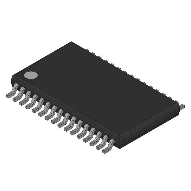
The 34903/4/5 is the second generation family of the System Basis Chip (SBC). It combines several features and enhances present module designs. The device works as an advanced power management unit for the MCU with additional integrated circuits such as sensors and CAN transceivers. It has a built-in enhanced high-speed CAN interface (ISO11898-2 and -5) with local and bus failure diagnostics, protection, and fail-safe operation modes. The SBC may include zero or one LIN 2.1 interface with LIN output pin switches. It includes up to four wake-up input pins that can also be configured as output drivers for flexibility. This device is powered by SMARTMOS technology. This device implements multiple Low-power (LP) modes, with very low-current consumption. In addition, the device is part of a family concept where pin compatibility adds versatility to module design. The 34903/4/5 also implements an innovative and advanced fail-safe state machine and concept solution. Features Voltage regulator for MCU, 3.3 V, part number selectable, with possibility of usage external PNP to extend current capability and share power dissipation Voltage, current, and temperature protection Extremely low quiescent current in LP modes Fully-protected embedded 5.0 V regulator for the CAN driver Multiple undervoltage detections to address various MCU specifications and system operation modes (i.e. cranking) Auxiliary 3.3 V SPI configurable regulator, for additional ICs, with overcurrent detection and undervoltage protection MUX output pin for device internal analog signal monitoring and power supply monitoring Advanced SPI, MCU, ECU power supply, and critical pins diagnostics and monitoring. Multiple wake-up sources in LP modes: CAN or LIN bus, I/O transition, automatic timer, SPI message, and VDD overcurrent detection. ISO11898-5 high-speed CAN interface compatibility for baud rates of 40 kb/s to 1.0 Mb/s Scalable product family of devices ranging from to 1 LIN, compatible to J2602-2 and LIN 2.1
Applications Industrial process control Automation Motor control RoboticsFreescale Semiconductor, Inc. reserves the right to change the detail specifications, as may be required, to permit improvements in the design of its products.
Simplified Application Diagrams................................................................................................................. 3 Device Variations....................................................................................................................................... 5 Internal Block Diagrams............................................................................................................................. 6 Pin Connections......................................................................................................................................... 8 Electrical Characteristics.......................................................................................................................... 12 Maximum Ratings.................................................................................................................................. 12 Static Electrical Characteristics............................................................................................................. 15 Dynamic Electrical Characteristics........................................................................................................ 23 Timing Diagrams................................................................................................................................... 26 Functional Description.............................................................................................................................. 31 Introduction............................................................................................................................................ 31 Functional Pin Description..................................................................................................................... 31 Functional Device Operation.................................................................................................................... 35 Mode and State Description.................................................................................................................. 35 LP Modes.............................................................................................................................................. 36 State Diagram........................................................................................................................................ 37 Mode Change........................................................................................................................................ 38 Watchdog Operation.............................................................................................................................. 38 Functional Block Operation Versus Mode............................................................................................. 40 Illustration of Device Mode Transitions................................................................................................. 41 Cyclic Sense Operation During LP Modes............................................................................................ 43 Behavior at Power Up and Power Down............................................................................................... 45 Fail-safe Operation................................................................................................................................... 47 CAN Interface........................................................................................................................................ 51 CAN Interface Description..................................................................................................................... 51 CAN Bus Fault Diagnostic..................................................................................................................... 54 LIN Block.................................................................................................................................................. 57 LIN Interface Description....................................................................................................................... 57 LIN Operational Modes.......................................................................................................................... 57 Serial Peripheral Interface........................................................................................................................ 59 High Level Overview.............................................................................................................................. 59 Detail Operation..................................................................................................................................... 60 Detail of Control Bits And Register Mapping......................................................................................... 63 Flags and Device Status........................................................................................................................ 78 Typical Applications................................................................................................................................. 85 Packaging................................................................................................................................................ 90
Analog Integrated Circuit Device Data Freescale SemiconductorVBAUX VCAUX VSUP1 VAUX VE VB VDD VSUP2 SAFE DBG GND VSENSE I/O-0 RST INT MOSI SCLK MISO CS MUX-OUT 5V-CAN TXD RXD TXD-L RXD-L
VBAUX VCAUX VSUP1 VAUX VE VB VDD VSUP2 SAFE DBG GND VSENSE I/O-0 RST INT MOSI SCLK MISO CS MUX-OUT 5V-CAN TXD RXD
Feature
- Voltage regulator for MCU, 5.0 or 3.3 V, part number selectable, with possibility of usage external PNP to extend current capability and share power dissipation
- Very low quiescent current in LP modes
- Fully protected embedded 5.0 V regulator for the CAN driver
- Multiple undervoltage detections to address various MCU specifications and system operation modes
- Auxiliary 5.0 or 3.3 V SPI configurable regulator, for additional ICs, with overcurrent detection and undervoltage protection
- MUX output pin for device internal analog signal monitoring and power supply monitoring
- Advanced SPI, MCU, ECU power supply, and critical pins diagnostics and monitoring.
- Multiple wake-up sources in LP modes: CAN or LIN bus, I/O transition, automatic timer, SPI message, and VDD overcurrent detection.
- ISO11898-5 high-speed CAN interface compatibility for baud rates of 40 kb/s to 1.0 Mb/s
- Scalable product family of devices ranging from 0 to 1 LIN, compatible to J2602-2 and LIN 2.1

