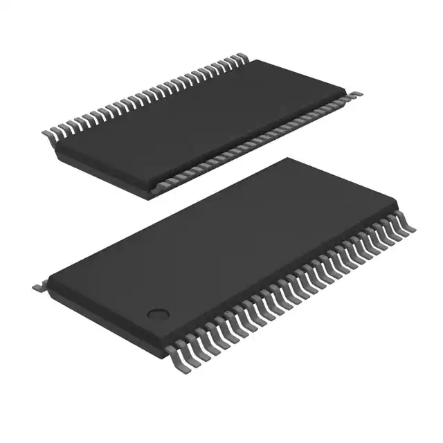
The 'ABT16833 consist of two noninverting 8-bit to 9-bit parity bus transceivers and are designed for communication between data buses. For each transceiver, when data is transmitted from the A bus to the B bus, an odd-parity bit is generated and output on the parity I/O pin (1PARITY or 2PARITY). When data is transmitted from the B bus to the A bus, 1PARITY (or 2PARITY) is configured as an input and combined with the B-input data to generate an active-low error flag if odd parity is not detected.
The error (1 or 2) output is configured as an open-collector output. The B-to-A parity-error flag is clocked into 1 (or 2) on the low-to-high transition of the clock (1CLK or 2CLK) input. 1 (or 2) is cleared (set high) by taking the clear (1 or 2) input low.
The output-enable ( and) inputs can be used to disable the device so that the buses are effectively isolated. When bothand are low, data is transferred from the A bus to the B bus and inverted parity is generated. Inverted parity is a forced error condition that gives the designer more system diagnostic capability.
To ensure the high-impedance state during power up or power down,should be tied to VCC through a pullup resistor; the minimum value of the resistor is determined by the current-sinking capability of the driver.
The SN54ABT16833 is characterized for operation over the full military temperature range of -55°C to 125°C. The SN74ABT16833DGGR is characterized for operation from -40°C to 85°C.
Feature
- Members of the Texas Instruments WidebusTM Family
- State-of-the-Art EPIC-IIBTM BiCMOS DesignSignificantly Reduces Power Dissipation
- Latch-Up Performance Exceeds 500 mA Per JEDEC Standard JESD-17
- Typical VOLP (Output Ground Bounce) < 1 V atVCC = 5 V, TA = 25°C
- Distributed VCC and GND Pin Configuration MinimizesHigh-Speed Switching Noise
- Flow-Through Architecture Optimizes PCB Layout
- High-Drive Outputs (-32-mA IOH, 64-mAIOL)
- Parity-Error Flag With Parity Generator/Checker
- Register for Storage of Parity-Error Flag
- Package Options Include Plastic 300-mil Shrink Small-Outline(DL) and Thin Shrink Small-Outline (DGG) Packages and 380-milFine-Pitch Ceramic Flat (WD) Package Using 25-mil Center-to-CenterSpacings


