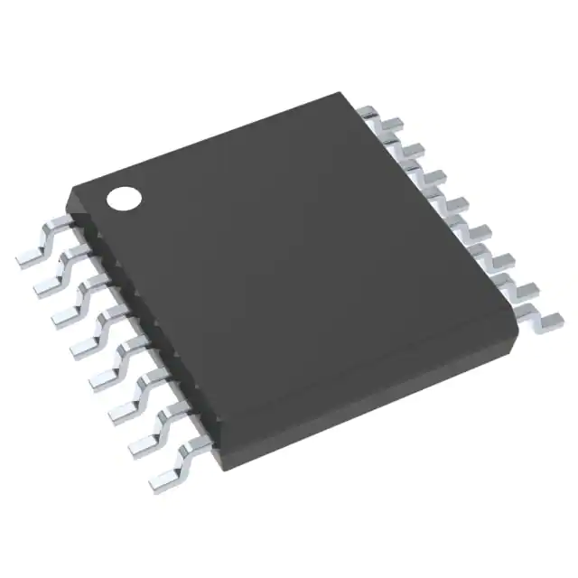
CD4521BPWRE4 consists of an oscillator section and 24 ripple-carry binary counter stages. The oscillator configuration(using IN1) allows design of either RC or crystal oscillator circuits. IN1 should be tied either HIGH or LOW when notin use. A HIGH on the RESET causes the counter to go to the all-0’s state and disables the oscillator. The count isadvanced on the negative transition of IN1 (and IN2). A time-saving test mode is described in the Functional Test SequenceTable and in Fig. 6.
The CD4521BPWRE4 types are supplied in 16-lead dual-in-line plastic packages (E suffix), 16-lead small-outline packages (M, M96, MT, and NSR suffixes), and 16-lead thin shrink small-outline packages (PW and PWR suffixes).
Feature
- Reset disables the RC oscillator for low-power standby condition
- VDD’ and VSS’ pins are brought out from the crystal oscillator to allow use of external resistors for low-power operation
- Maximum input current of 1 μA at 18 V over full package-temperature range:
100 nA at 18 V and 25°C - Common reset
- 100% tested for 20-V quiescent current
- 5, 10 and 15 V parametric ratings
- Standardized symmetrical output characteristics
- Meets all requirements of JEDEC Tentative Standard No. 13B, "Standard Specifications for Description of ’B’ SeriesCMOS Devices"


