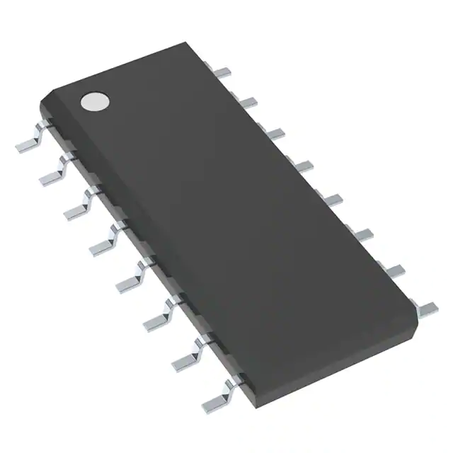
These hex buffers and line drivers are designed specifically to improve both the performance and density of 3-statememory address drivers, clock drivers, and bus-oriented receivers and transmitters. The ’HC365 devices containsix independent buffers/drivers with dual-gated output-enable (OE1\ and OE2\) inputs. When OE1\ and OE2\ are both low,the deviceS pass noninverted data from the A inputs to the Y outputs. If either (or both) output-enable terminal(s) ishigh, the outputs are in the high-impedance state.
Feature
- Wide Operating Voltage Range of 2 V to 6 V
- High-Current 3-State Outputs Drive Bus Lines, Buffer Memory Address Registers, or Drive Up To 15 LSTTL Loads
- True Outputs
- Low Power Consumption, 80-μA Max ICC
- Typical tpd = 10 ns
- ±6-mA Output Drive at 5 V
- Low Input Current of 1 μA Max


