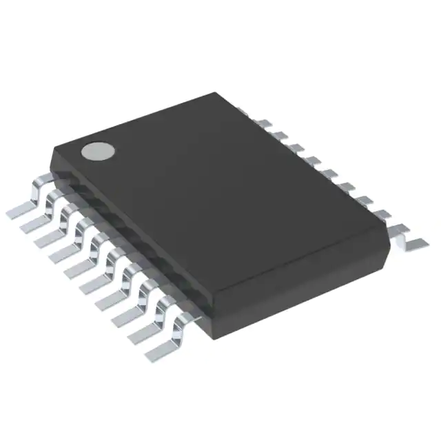
The 'ABT2952A transceivers consist of two 8-bit back-to-back registers that store data flowing in both directions between two bidirectional buses. Data on the A or B bus is stored in the registers on the low-to-high transition of the clock (CLKAB or CLKBA) input provided that the clock-enable (CLKENAB\ or CLKENBA\) input is low. Taking the output-enable (OEAB\ or OEBA\) input low accesses the data on either port.
To ensure the high-impedance state during power up or power down, OE\ should be tied to VCC through a pullup resistor; the minimum value of the resistor is determined by the current-sinking capability of the driver.
The SN54ABT2952A is characterized for operation over the full military temperature range of -55°C to 125°C. The SN74ABT2952ANSRG4 is characterized for operation from -40°C to 85°C.
Feature
- State-of-the-ArtEPIC-II BTM BiCMOS Design Significantly Reduces Power Dissipation
- Two 8-Bit Back-to-Back Registers Store Data Flowing in Both Directions
- Noninverting Outputs
- Typical VOLP (Output Ground Bounce) < 1 V at VCC = 5 V, TA = 25°C
- Latch-Up Performance Exceeds 500 mA Per JESD 17
- ESD Protection Exceeds 2000 V Per MIL-STD-883, Method 3015; Exceeds 200 V Using Machine Model (C = 200 pF, R = 0)
- Package Options Include Plastic Small-Outline (DW), Shrink Small-Outline (DB), and Thin Shrink Small-Outline (PW) Packages, Ceramic Chip Carriers (FK), Ceramic Flat (W) Package, and Plastic (NT) and Ceramic (JT) DIPs


