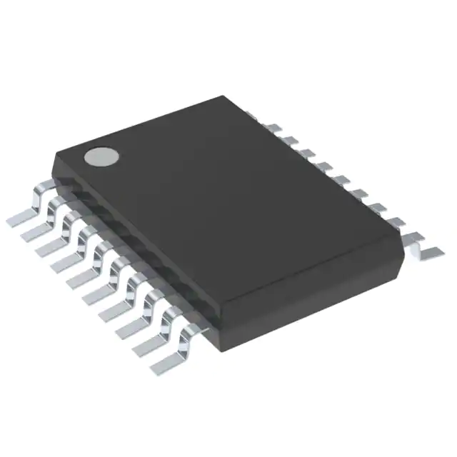
The SN74LV541ATNSG4 is designed for 4.5-V to 5.5-V VCC operation. The inputs are TTL-voltage compatible, which allows them to be interfaced with bipolar outputs and 3.3-V devices. The device also can be used to translate from 3.3 V to 5 V.
This device is ideal for driving bus lines or buffer memory address registers. It features inputs and outputs on opposite sides of the package to facilitate printed circuit board layout.
The 3-state control gate is a two-input AND gate with active-low inputs so that, if either output-enable (OE1 or OE2) input is high, all corresponding outputs are in the high-impedance state. The outputs provide noninverted data when they are not in the high-impedance state.
To ensure the high-impedance state during power up or power down, OE shall be tied to VCC through a pullup resistor; the minimum value of the resistor is determined by the current-sinking capability of the driver.
This device is fully specified for partial-power-down applications using Ioff. The Ioff circuitry disables the outputs, preventing damaging current backflow through the device when it is powered down.
Feature
- Inputs Are TTL-Voltage Compatible
- 4.5-V to 5.5-V VCC Operation
- Typical tpd of 4 ns at 5 V
- Typical VOLP (Output Ground Bounce)
<0.8 V at VCC = 5 V, TA = 25°C - Typical VOHV (Output VOH Undershoot)
>2.3 V at VCC = 5 V, TA = 25°C - Supports Mixed-Mode Voltage Operation on All Ports
- Ioff Supports Partial-Power-Down Mode Operation
- Latch-Up Performance Exceeds 250 mA Per JESD 17
- ESD Protection Exceeds JESD 22
- 2000-V Human-Body Model (A114-A)
- 200-V Machine Model (A115-A)
- 1000-V Charged-Device Model (C101)


