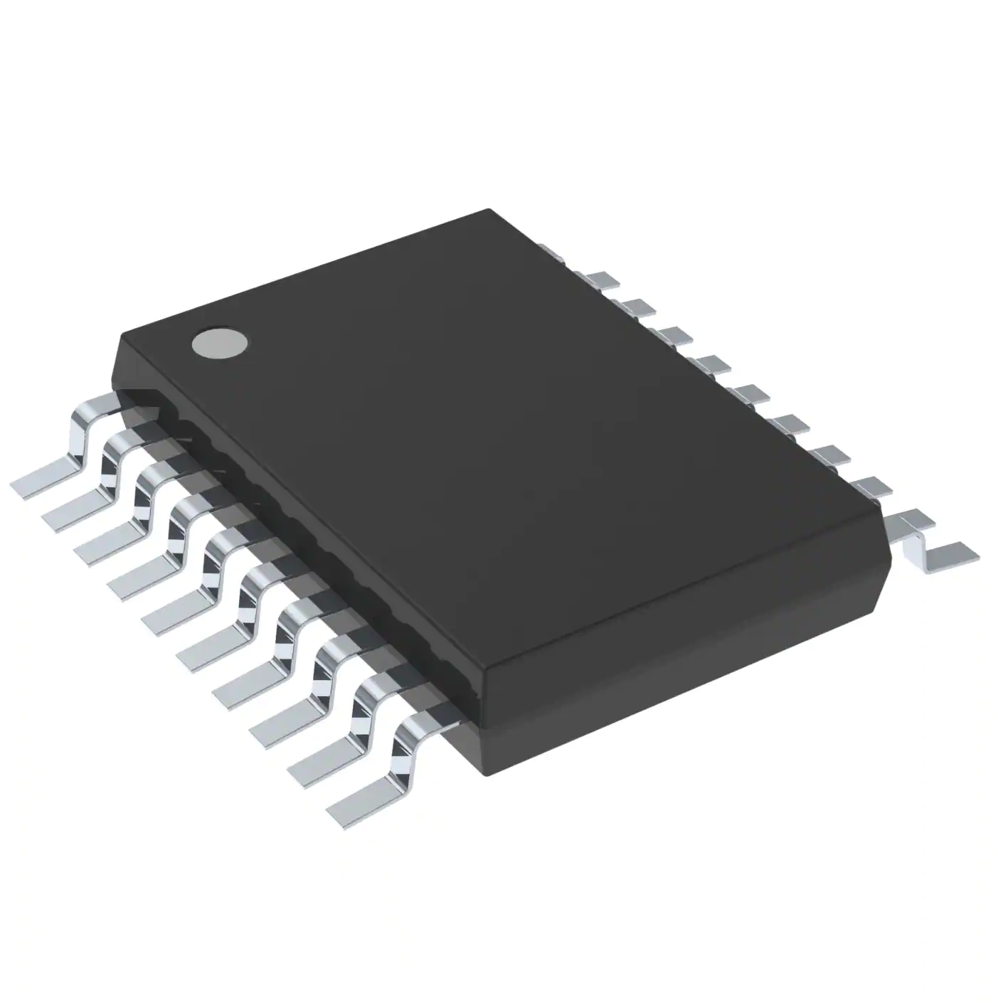
The SN54LVC646A octal bus transceiver and register is designed for 2.7-V to 3.6-V VCC operation, and the SN74LVC646ADWRG4 octal bus transceiver and register is designed for 1.65-V to 3.6-V VCC operation.
These devices consist of bus-transceiver circuits, D-type flip-flops, and control circuitry arranged for multiplexed transmission of data directly from the input bus or from the internal registers. Data on the A or B bus is clocked into the registers on the low-to-high transition of the appropriate clock (CLKAB or CLKBA) input. Figure 1 illustrates the four fundamental bus-management functions that are performed with the ’LVC646A devices.
Output-enable (OE)\ and direction-control (DIR) inputs control the transceiver functions. In the transceiver mode, data present at thehigh-impedance port is stored in either register or in both.
The select-control (SAB and SBA) inputs can multiplex stored and real-time (transparent mode) data. DIR determines which bus receives data when OE\ is low. In the isolation mode (OE\ high), A data is stored in one register and B data can be stored in the other register.
When an output function is disabled, the input function is still enabled and can be used to store and transmit data. Only one of the two buses, A or B, can be driven at a time.
Inputs can be driven from either 3.3-V or 5-V devices. This feature allows the use of these devices as translators in a mixed 3.3-V/5-V system environment.
These devices are fully specified for partial-power-down applications using Ioff. The Ioff circuitry disables the outputs, preventing damaging current backflow through the device when it is powered down.
To ensure the high-impedance state during power up or power down, OE\ should be tied to VCC through a pullup resistor; the minimum value of the resistor is determined by the current-sinking capability of the driver.
Feature
- Operate From 1.65 V to 3.6 V
- Inputs Accept Voltages to 5.5 V
- Max tpd of 7.4 ns at 3.3 V
- Typical VOLP(Output Ground Bounce)
<0.8 V at VCC = 3.3 V, TA = 25°C - Typical VOHV (Output VOH Undershoot)
>2 V at VCC = 3.3 V, TA = 25°C - Supports Mixed-Mode Signal Operation on All Ports (5-V Input/Output Voltage With 3.3-V VCC)
- Ioff Supports Partial-Power-Down Mode Operation
- Latch-Up Performance Exceeds 250 mA Per JESD 17
- ESD Protection Exceeds JESD 22
- 2000-V Human-Body Model (A114-A)
- 200-V Machine Model (A115-A)
- 1000-V Charged-Device Model (C101)


