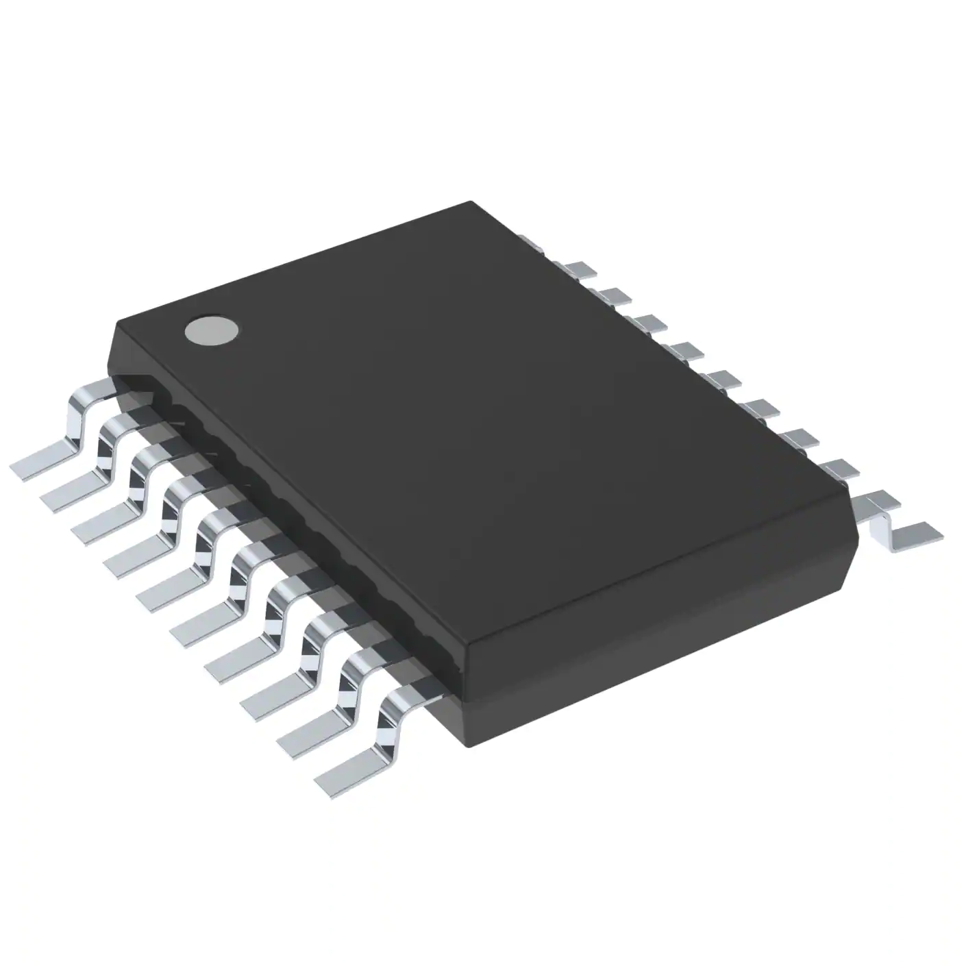
These bus transceivers and registers are designed specifically for low-voltage (3.3-V) VCC operation, but with the capability to provide a TTL interface to a 5-V system environment.
The ’LVTH652 devices consist of bus-transceiver circuits, D-type flip-flops, and control circuitry arranged for multiplexed transmission of data directly from the data bus or from the internal storage registers.
Output-enable (OEAB and OEBA\) inputs are provided to control the transceiver functions. Select-control (SAB and SBA) inputs are provided to select whether real-time or stored data is transferred. The circuitry used for select control eliminates the typical decoding glitch that occurs in a multiplexer during the transition between real-time and stored data. A low input selects real-time data and a high input selects stored data. Figure 1 illustrates the four fundamental bus-management functions that can be performed with the ’LVTH652 devices.
Data on the A or B data bus, or both, can be stored in the internal D-type flip-flops by low-to-high transitions at the appropriate clock (CLKAB or CLKBA) inputs, regardless of the select- or enable-control pins. When SAB and SBA are in the real-time transfer mode, it is possible to store data without using the internal D-type flip-flops by simultaneously enabling OEAB and OEBA\. In this configuration, each output reinforces its input; therefore, when all other data sources to the two sets of bus lines are at high impedance, each set of bus lines remains at its last state.
Active bus-hold circuitry is provided to hold unused or floating data inputs at a valid logic level. Use of pullup or pulldown resistors with the bus-hold circuitry is not recommended.
When VCC is between 0 and 1.5 V, the device is in the high-impedance state during power up or power down. However, to ensure the high-impedance state above 1.5 V, OE\ should be tied to VCC through a pullup resistor and OE should be tied to GND through a pulldown resistor; the minimum value of the resistor is determined by the current-sinking/current-sourcing capability of the driver.
This device is fully specified for hot-insertion applications using Ioff and power-up 3-state. The Ioff circuitry disables the outputs, preventing damaging current backflow through the device when it is powered down. The power-up 3-state circuitry places the outputs in the high-impedance state during power up and power down, which prevents driver conflict.
Feature
- Support Mixed-Mode Signal Operation (5-V Input and Output Voltages With 3.3-V VCC)
- Support Unregulated Battery Operation Down to 2.7 V
- Typical VOLP (Output Ground Bounce)
<0.8 V at VCC = 3.3 V, TA = 25°C - Ioff and Power-Up 3-State Support Hot Insertion
- Bus Hold on Data Inputs Eliminates the Need for External Pullup/Pulldown Resistors
- Latch-Up Performance Exceeds 500 mA Per JESD 17
- ESD Protection Exceeds JESD 22
- 2000-V Human-Body Model (A114-A)
- 200-V Machine Model (A115-A)


