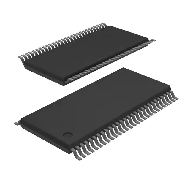
A FIFO memory is a storage device that allows data to be written into and read from its array at independent data rates. The SN74ALVC7814-25DL is an 18-bit FIFO with high speed and fast access times. Data is processed at rates up to 40 MHz with access times of 18 ns in a bit-parallel format. These memories are designed for 3-V to 3.6-V VCC operation.
Data is written into memory on a low-to-high transition of the load clock (LDCK) and is read out on a low-to-high transition of the unload clock (UNCK). The memory is full when the number of words clocked in exceeds the number of words clocked out by 64. When the memory is full, LDCK has no effect on the data residing in memory. When the memory is empty, UNCK has no effect.
Status of the FIFO memory is monitored by the full (FULL\), empty (EMPTY\), half-full (HF), and almost- full/almost-empty (AF/AE) flags. The FULL\ output is low when the memory is full and high when the memory is not full. The EMPTY\ output is low when the memory is empty and high when it is not empty. The HF output is high whenever the FIFO contains 32 or more words and low when it contains 31 or fewer words. The AF/AE status flag is a programmable flag. The first one or two low-to-high transitions of LDCK after reset are used to program the almost-empty offset value (X) and the almost-full offset value (Y) if program enable (PEN\) is low. The AF/AE flag is high when the FIFO contains X or fewer words or (64 - Y) or more words. The AF/AE flag is low when the FIFO contains between (X + 1) and (63 - Y) words.
A low level on the reset (RESET\) resets the internal stack pointers and sets FULL\ high, AF/AE high, HF low, and EMPTY\ low. The Q outputs are not reset to any specific logic level. The FIFO must be reset on power up. The first word loaded into empty memory causes EMPTY\ to go high and the data to appear on the Q outputs. The data outputs are in the high-impedance state when the output-enable (OE\) is high.
The SN74ALVC7814-25DL is characterized for operation from 0°C to 70°C.
Feature
- Member of the Texas Instruments WidebusTM Family
- Low-Power Advanced CMOS Technology
- Operates From 3-V to 3.6-V VCC
- Load Clock and Unload Clock Can Be Asynchronous or Coincident
- Full, Empty, and Half-Full Flags
- Programmable Almost-Full/Almost-Empty Flag
- Fast Access Times of 18 ns With a 50-pF Load and All Data Outputs Switching Simultaneously
- Data Rates up to 40 MHz
- 3-State Outputs
- Pin-to-Pin Compatible With SN74ACT7804, SN74ACT7806, and SN74ACT7814
- Packaged in Shrink Small-Outline 300-mil Package Using 25-mil Center-to-Center Spacing


