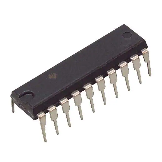
This 80-bit active-element memory is a monolithic Schottky-clamped transistor-transistor logic (STTL) array organized as 16 words by 5 bits. A memory system using the SN74S225N easily can be expanded in multiples of 48 words or of 10 bits as shown in Figure 3. The 3-state outputs controlled by a single output-enable (OE\) input make bus connection and multiplexing easy.
A first-in, first-out (FIFO) memory is a storage device that allows data to be written into and read from its array at independent data rates. This FIFO is designed to process data at rates from dc to 10MHz in a bit-parallel format, word by word.
Reading or writing is done independently, utilizing separate asynchronous data clocks. Data can be written into the array on the low-to-high transition of either load-clock (CLKA, CLKB) input. Data can be read out of the array on the low-to-high transition of the unload-clock (UNCK IN) input (normally high). Writing data into the FIFO can be accomplished in one of two ways:
- In applications not requiring a gated clock control, best results are achieved by applying the clock input to one of the clocks while tying the other clock input high.
- In applications needing a gated clock, the load clock (gate control) must be high for the FIFO to load on the next clock pulse.
CLKA and CLKB can be used interchangeably for either clock gate control or clock input.
Status of the SN74S225N is provided by three outputs. The input-ready (IR) output monitors the status of the last word location and signifies when the memory is full. This output is high whenever the memory is available to accept any data. The unload-clock (UNCK OUT) output also monitors the last word location. This output generates a low-logic-level pulse (synchronized to the internal clock pulse) when the location is vacant. The third status output, output ready (OR), is high when the first word location contains valid data and UNCK IN is high. When UNCK IN goes low, OR will go low and stay low until new valid data is in the first word position. The first word location is defined as the location from which data is provided to the outputs.
The data outputs are noninverted with respect to the data inputs and are 3-state, with a common control input (OE\). When OE\ is low, the data outputs are enabled to function as totem-pole outputs. A high logic level forces each data output to a high-impedance state while all other inputs and outputs remain active.The clear (CLR\) input invalidates all data stored in the memory array by clearing the control logic and setting OR to a low logic level on the high-to-low transition of a low-active pulse.
The SN74S225N is characterized for operation from 0°C to 70°C.
Feature
- Independent Asychronous Inputs and Outputs
- 16 Words by 5 Bits
- DC to 10-MHz Data Rate
- 3-State Outputs
- Packaged in Standard Plastic 300-mil DIPs


