久芯网
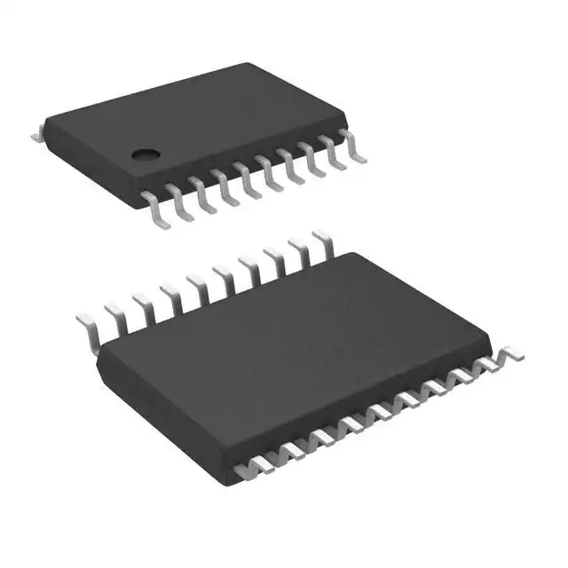
NLVHCT244ADWR2G
收藏

NLVHCT244ADWR2G

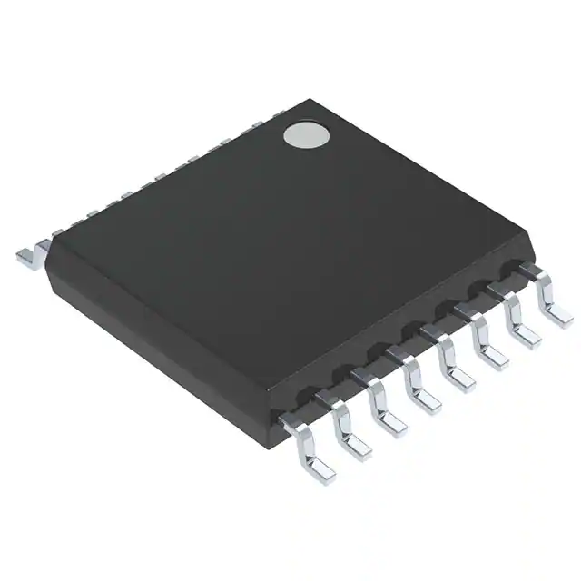
  • 描述:逻辑类型: 缓冲区,非反相 电源电压: 4.5伏~5.5伏 每个元件的位数: four 供应商设备包装: 20-SOIC 工作温度: -55摄氏度~125摄氏度(TA) 安装类别: 表面安装
  • 品牌: 安盛美 (onsemi)
  • 交期:5-7 工作日
渠道:
  • 自营
  • 得捷
  • 贸泽

起订量: 1

  • 库存: 0
  • 单价: ¥8.45102
  • 数量:
    - +
  • 总计: ¥8.45
在线询价

温馨提示: 请填写以下信息,以便客户代表及时与您沟通联系。

规格参数

  • 制造厂商 安盛美 (onsemi)
  • 逻辑类型 缓冲区,非反相
  • 元件数量 two
  • 输出类别 三态
  • 输入类别 -
  • 电源电压 4.5伏~5.5伏
  • 安装类别 表面安装
  • 每个元件的位数 four
  • 包装/外壳 20-SOIC(0.295“,7.50毫米宽)
  • 部件状态 过时的
  • 供应商设备包装 20-SOIC
  • 输出高电流, 输出低电流 6毫安, 6毫安
  • 工作温度 -55摄氏度~125摄氏度(TA)

NLVHCT244ADWR2G 产品详情

High-Performance Silicon-Gate CMOSThe NLVHCT244ADWR2G is identical in pinout to the LS244. This device may be used as a level converter for interfacing TTL or NMOS outputs to High-Speed CMOS inputs. The HCT244A is an octal noninverting buffer line driver line receiver designed to be used with 3-state memory address drivers, clock drivers, and other bus-oriented systems. The device has non-inverted outputs and two active-low output enables. The HCT244A is the noninverting version of the HCT240. See also HCT241.

Feature

  • Output Drive Capability: 15 LSTTL Loads
  • TTL NMOS-Compatible Input Levels
  • Outputs Directly Interface to CMOS, NMOS, and TTL
  • Operating Voltage Range: 4.5 to 5.5 V
  • Low Input Current: 1 mA
  • In Compliance with the Requirements Defined by JEDEC Standard No. 7A
  • Chip Complexity: 112 FETs or 28 Equivalent Gates
  • Pb-Free Packages are Available


(Picture: Pinout)

NLVHCT244ADWR2G所属分类:逻辑接收/发送/驱动/缓冲器,NLVHCT244ADWR2G 由 安盛美 (onsemi) 设计生产,可通过久芯网进行购买。NLVHCT244ADWR2G价格参考¥8.451016,你可以下载 NLVHCT244ADWR2G中文资料、PDF数据手册、Datasheet数据手册功能说明书,可查询NLVHCT244ADWR2G规格参数、现货库存、封装信息等信息!

安盛美 (onsemi)

安盛美 (onsemi)

onsemi正在推动节能创新,使客户能够减少全球能源使用。该公司提供全面的节能电源和信号管理、逻辑、离散和定制解决方案组合,以帮助设计工程师解决其在汽车、通信、计算、消费、工业、LED照明、医疗、军事/...

展开
会员中心 微信客服
客服
回到顶部