The NLVVHC1GT126DF1G is a single gate noninverting 3-state buffer fabricated with silicon gate CMOS technology. It achieves high speed operation similar to equivalent Bipolar Schottky TTL while maintaining CMOS low power dissipation. The NLVVHC1GT126DF1G requires the 3-state control input (OE(bar)) to be set Low to place the output into the high impedance state. The device input is compatible with TTL-type input thresholds and the output has a full 5V CMOS level output swing. The input protection circuitry on this device allows overvoltage tolerance on the input, allowing the device to be used as a logic-level translator from 3.0V CMOS logic to 5.0V CMOS Logic or from 1.8V CMOS logic to 3.0V CMOS Logic while operating at the high-voltage power supply. The NLVVHC1GT126DF1G input structure provides protection when voltages up to 5.5V are applied, regardless of the supply voltage. This allows the NLVVHC1GT126DF1G to be used to interface 5V circuits to 3V circuits. The output structures also provide protection when VCC = 0V. These input and output structures help prevent device destruction caused by supply voltage - input/output voltage mismatch, battery backup, hot insertion, etc.
Feature
- High Speed: tPD = 3.5ns (Typ) at V CC = 5V
- Low Power Dissipation: ICC = 1µA (Max) at TA = 25°C
- TTL-Compatible Inputs: VIL = 0.8V; VIH = 2.0V
- CMOS-Compatible Outputs: VOH > 0.8VCC ; VOL < 0.1VCC @Load
- Power Down Protection Provided on Inputs and Outputs
- Balanced Propagation Delays
- Pin and Function Compatible with Other Standard Logic Families
- Chip Complexity: FETs = ≤ 100
- Pb-Free Packages are Available
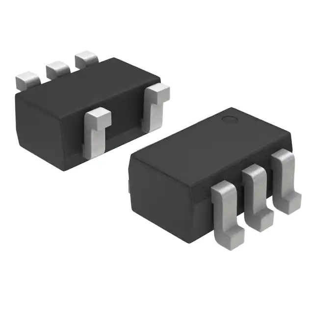
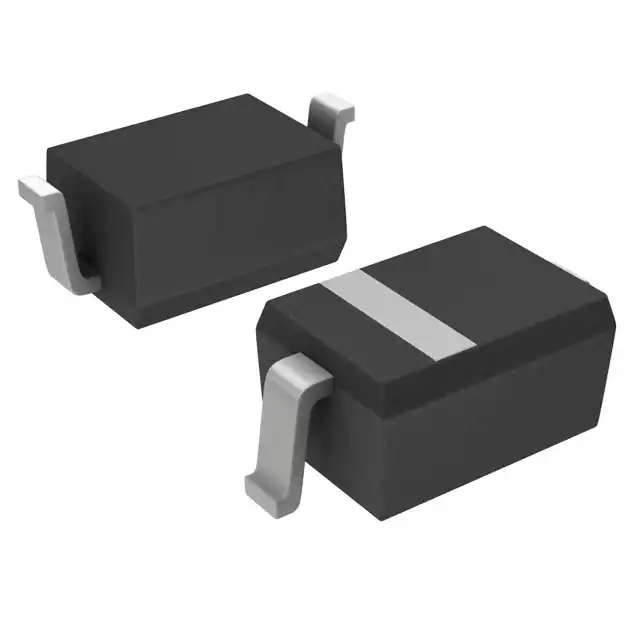
(Picture: Pinout)