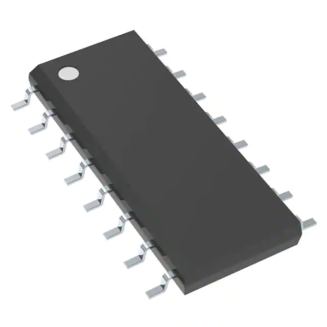
The ’HC365, ’HCT365, and ’HC366 silicon gate CMOS three-state buffers are general purpose high-speed non-inverting and inverting buffers. They have high drive current outputs which enable high speed operation even when driving large bus capacitances. These circuits possess the low power dissipation of CMOS circuitry, yet have speeds comparable to low power Schottky TTL circuits. Both circuits are capable of driving up to 15 low power Schottky inputs.
The ’HC365 and ’HCT365 are non-inverting buffers, whereas the ’HC366 is an inverting buffer. These devices have two three-state control inputs (OE1\ and OE2\) which are NORed together to control all six gates.
The ’HCT365 logic families are speed, function and pin compatible with the standard LS logic family.
Feature
- Buffered Inputs
- High Current Bus Driver Outputs
- Typical Propagation Delay tPLH, tPHL = 8ns at VCC =5V, CL = 15pF, TA = 25°C
- Fanout (Over Temperature Range)
- Standard Outputs...10 LSTTL Loads
- Bus Driver Outputs...15 LSTTL Loads
- Wide Operating Temperature Range... –55°C to 125°C
- Balanced Propagation Delay and Transition Times
- Significant Power Reduction Compared to LSTTL Logic ICs
- HC Types
- 2V to 6V Operation
- High Noise Immunity: NIL = 30%, NIH = 30% of VCC at VCC = 5V
- HCT Types
- 4.5V to 5.5V Operation
- Direct LSTTL Input Logic Compatibility, VIL = 0.8V (Max), VIH = 2V (Min)
- CMOS Input Compatibility, Il 1μA at VOL, VOH


