All trademarks are the property of their respective owners.
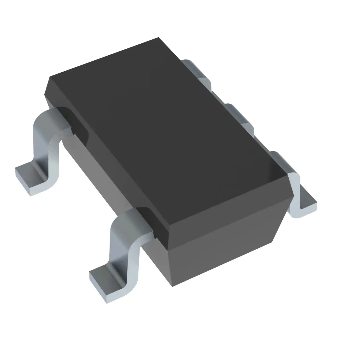
DescriptionThe SN74LVC1G79DBVT device is a singlepositive-edge-triggered D-type flip-flop that is designed for 1.65-V to 5.5-VVCC operation.
When data at the data (D) input meets the setup time requirement, the data is transferredto the Q output on the positive-going edge of the clock pulse. Clock triggering occurs at a voltagelevel and is not directly related to the rise time of the clock pulse. Following the hold-timeinterval, data at the D input can be changed without affecting the level at the output.
NanoFree? packagetechnology is a major breakthrough in IC packaging concepts, using the die as the package.
This device is fully specified for partial-power-down applications usingIoff. The Ioff circuitry disables the outputs whenthe device is powered down. This inhibits current backflow into the device which prevents damage tothe device.
Feature
- Available in the Texas Instruments NanoFree? Package
- Latch-Up Performance Exceeds 100 mAPer JESD 78, Class II
- ESD Protection Exceeds JESD 22
- 2000-V Human-Body Model (A114-A)
- 200-V Machine Model (A115-A)
- 1000-V Charged-Device Model (C101)
- Supports 5-VVCC Operation
- Inputs Accept Voltages to 5.5 V
- Supports Down Translation to VCC
- Maxtpd of 6 ns at 3.3 V and 50 pF load
- Low Power Consumption, 10-μA Max ICC
- ±24-mA Output Drive at 3.3 V
- Ioff supports Partial-Power-Down Mode and Back-DriveProtection
All trademarks are the property of their respective owners.
DescriptionThe SN74LVC1G79 device is a singlepositive-edge-triggered D-type flip-flop that is designed for 1.65-V to 5.5-VVCC operation.
When data at the data (D) input meets the setup time requirement, the data is transferredto the Q output on the positive-going edge of the clock pulse. Clock triggering occurs at a voltagelevel and is not directly related to the rise time of the clock pulse. Following the hold-timeinterval, data at the D input can be changed without affecting the level at the output.
NanoFree? packagetechnology is a major breakthrough in IC packaging concepts, using the die as the package.
This device is fully specified for partial-power-down applications usingIoff. The Ioff circuitry disables the outputs whenthe device is powered down. This inhibits current backflow into the device which prevents damage tothe device.


