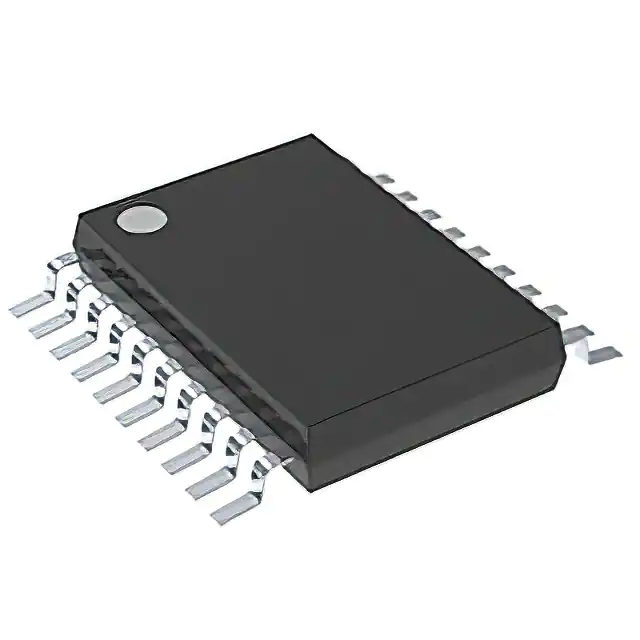
This octal edge-triggered D-type flip-flop is designed for 1.65-V to 3.6-V VCC operation.
The SN74ALVCH374PW is particularly suitable for implementing buffer registers, I/O ports, bidirectional bus drivers, and working registers. On the positive transition of the clock (CLK) input, the Q outputs are set to the logic levels at the data (D) inputs.
A buffered output-enable (OE)\ input can be used to place the eight outputs in either a normal logic state (high or low logic levels) or the high-impedance state. In the high-impedance state, the outputs neither load nor drive the bus lines significantly. The high-impedance state and increased drive provide the capability to drive bus lines without interface or pullup components.
OE\ does not affect internal operations of the latch. Old data can be retained or new data can be entered while the outputs are in the high-impedance state.
To ensure the high-impedance state during power up or power down, OE\ should be tied to VCC through a pullup resistor; the minimum value of the resistor is determined by the current-sinking capability of the driver.
Active bus-hold circuitry holds unused or undriven inputs at a valid logic state. Use of pullup or pulldown resistors with the bus-hold circuitry is not recommended.
Feature
- Operates From 1.65 V to 3.6 V
- Max tpd of 3.6 ns at 3.3 V
- ±24-mA Output Drive at 3.3 V
- Bus Hold on Data Inputs Eliminates the Need for External Pullup/Pulldown Resistors
- Latch-Up Performance Exceeds 100 mA Per JESD 78, Class II
- ESD Protection Exceeds JESD 22
- 2000-V Human-Body Model (A114-A)
- 200-V Machine Model (A115-A)
- 1000-V Charged-Device Model (C101)


