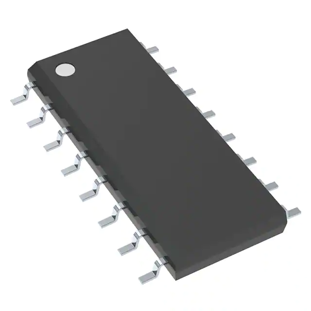
Data sheet acquired from Harris Semiconductor
DescriptionThe ’HC173 and ’HCT173 high speed three-state quad Dtype flip-flops are fabricated with silicon gate CMOS technology. They possess the low power consumption of standard CMOS Integrated circuits, and can operate at speeds comparable to the equivalent low power Schottky devices. The buffered outputs can drive 15 LSTTL loads. The large output drive capability and three-state feature make these parts ideally suited for interfacing with bus lines in bus oriented systems.
The four D-type flip-flops operate synchronously from a common clock. The outputs are in the three-state mode when either of the two output disable pins are at the logic "1" level. The input ENABLES allow the flip-flops to remain in their present states without having to disrupt the clock If either of the 2 input ENABLES are taken to a logic "1" level, the Q outputs are fed back to the inputs, forcing the flip-flops to remain in the same state. Reset is enabled by taking the MASTER RESET (MR) input to a logic "1" level. The data outputs change state on the positive going edge of the clock.
The ’HCT173 logic family is functionally, as well as pin compatible with the standard LS logic family.
Feature
- Three-State Buffered Outputs
- Gated Input and Output Enables
- Fanout (Over Temperature Range)
- Standard Outputs...10 LSTTL Loads
- Bus Driver Outputs...15 LSTTL Loads
- Wide Operating Temperature Range... –55°C to 125°C
- Balanced Propagation Delay and Transition Times
- Significant Power Reduction Compared to LSTTL Logic ICs
- HC Types
- 2V to 6V Operation
- High Noise Immunity: NIL = 30%, NIH = 30% of VCC at VCC = 5V
- HCT Types
- 4.5V to 5.5V Operation
- Direct LSTTL Input Logic Compatibility, VIL = 0.8V (Max), VIH = 2V (Min)
- CMOS Input Compatibility, Il1μA at VOL, VOH
Data sheet acquired from Harris Semiconductor
DescriptionThe ’HC173 and ’HCT173 high speed three-state quad Dtype flip-flops are fabricated with silicon gate CMOS technology. They possess the low power consumption of standard CMOS Integrated circuits, and can operate at speeds comparable to the equivalent low power Schottky devices. The buffered outputs can drive 15 LSTTL loads. The large output drive capability and three-state feature make these parts ideally suited for interfacing with bus lines in bus oriented systems.
The four D-type flip-flops operate synchronously from a common clock. The outputs are in the three-state mode when either of the two output disable pins are at the logic "1" level. The input ENABLES allow the flip-flops to remain in their present states without having to disrupt the clock If either of the 2 input ENABLES are taken to a logic "1" level, the Q outputs are fed back to the inputs, forcing the flip-flops to remain in the same state. Reset is enabled by taking the MASTER RESET (MR) input to a logic "1" level. The data outputs change state on the positive going edge of the clock.
The ’HCT173 logic family is functionally, as well as pin compatible with the standard LS logic family.


