All trademarks are the property of their respective owners.
DescriptionThe AUP family is TI’s premier solution to the industry’s low-power needs inbattery-powered portable applications. This family assures a very-low static and dynamic powerconsumption across the entire VCC range of 0.8 V to 3.6 V, thus resulting inan increased battery life. The AUP devices also maintain excellent signal integrity.
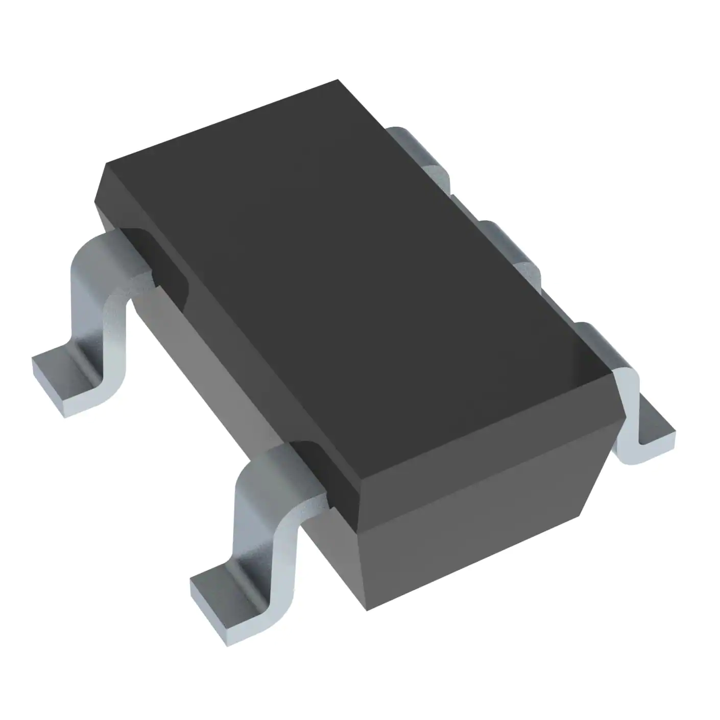
The SN74AUP1G79DBVT is a single positive-edge-triggered D-type flip-flop. When data at thedata (D) input meets the setup-time requirement, the data is transferred to the Q output on thepositive-going edge of the clock pulse. Clock triggering occurs at a voltage level and is notdirectly related to the rise time of the clock pulse. Following the hold-time interval, data at theD input can be changed without affecting the levels at the outputs.
NanoStar? package technology is a major breakthrough in IC packaging concepts, using thedie as the package.
The SN74AUP1G79DBVT device is fully specified for partial-power-down applications usingIoff. The Ioff circuitry disables the outputs whenthe device is powered down. This inhibits current backflow into the device which prevents damage tothe device.
Feature
- Available in the Texas Instruments NanoStar? Package
- Low Static-Power Consumption:ICC = 0.9 μA Maximum
- Low Dynamic-Power Consumption: Cpd = 3 pF Typical at 3.3 V
- Low Input Capacitance: Ci = 1.5 pF Typical
- Low Noise: Overshoot and Undershoot< 10% of VCC
- Ioff Supports Partial Power-Down-Mode Operation
- Input Hysteresis Allows Slow Input Transition and Better Switching Noise Immunityat the Input(Vhys = 250 mV Typical at 3.3 V)
- Wide Operating VCC Range of 0.8 V to 3.6 V
- Optimized for 3.3-V Operation
- 3.6-V I/O Tolerant to Support Mixed-Mode Signal Operation
- tpd = 4 ns Maximum at 3.3 V
- Suitable for Point-to-Point Applications
- Latch-Up Performance Exceeds 100 mA Per JESD 78, Class II
- ESD Performance Tested Per JESD 22
- 2000-V Human-Body Model(A114-B, Class II)
- 1000-V Charged-Device Model (C101)
All trademarks are the property of their respective owners.
DescriptionThe AUP family is TI’s premier solution to the industry’s low-power needs inbattery-powered portable applications. This family assures a very-low static and dynamic powerconsumption across the entire VCC range of 0.8 V to 3.6 V, thus resulting inan increased battery life. The AUP devices also maintain excellent signal integrity.
The SN74AUP1G79 is a single positive-edge-triggered D-type flip-flop. When data at thedata (D) input meets the setup-time requirement, the data is transferred to the Q output on thepositive-going edge of the clock pulse. Clock triggering occurs at a voltage level and is notdirectly related to the rise time of the clock pulse. Following the hold-time interval, data at theD input can be changed without affecting the levels at the outputs.
NanoStar? package technology is a major breakthrough in IC packaging concepts, using thedie as the package.
The SN74AUP1G79 device is fully specified for partial-power-down applications usingIoff. The Ioff circuitry disables the outputs whenthe device is powered down. This inhibits current backflow into the device which prevents damage tothe device.


