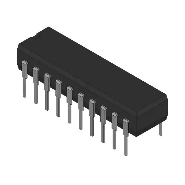
These 8-bit flip-flops feature 3-state outputs designed specifically for driving highly capacitive or relatively low-impedance loads. They are particularly suitable for implementing buffer registers, I/O ports, bidirectional bus drivers, and working registers.
The eight flip-flops of the ′F374 are edge-triggered D-type flip-flops. On the positive transition of the clock (CLK) input, the Q outputs are set to the logic levels that were set up at the data (D) inputs.
A buffered output enable () input can be used to place the eight outputs in either a normal logic state (high or low) or a high-impedance state. In the high-impedance state, the outputs neither load nor drive the bus lines significantly. The high-impedance state and the increased drive provide the capability to drive bus lines without need for interface or pullup components.
The output enable () input does not affect internal operations of the flip-flop. Old data can be retained or new data can be entered while the outputs are in the high-impedance state.
The SN74F374NSR is available in TI's shrink small-outline package (DB), which provides the same I/O pin count and functionality of standard small-outline packages in less than half the printed-circuit-board area.
The SN54F374 is characterized for operation over the full military temperature range of -55°C to 125°C. The SN74F374NSR is characterized for operation from 0°C to 70°C.
Feature
- Eight D-Type Flip-Flops in a Single Package
- 3-State Bus-Driving True Outputs
- Full Parallel Access for Loading
- Buffered Control Inputs
- Package Options Include Plastic Small-Outline (SOIC) andShrink Small-Outline (SSOP) Packages, Ceramic Chip Carriers, andPlastic and Ceramic DIPs
These 8-bit flip-flops feature 3-state outputs designed specifically for driving highly capacitive or relatively low-impedance loads. They are particularly suitable for implementing buffer registers, I/O ports, bidirectional bus drivers, and working registers.
The eight flip-flops of the ′F374 are edge-triggered D-type flip-flops. On the positive transition of the clock (CLK) input, the Q outputs are set to the logic levels that were set up at the data (D) inputs.
A buffered output enable () input can be used to place the eight outputs in either a normal logic state (high or low) or a high-impedance state. In the high-impedance state, the outputs neither load nor drive the bus lines significantly. The high-impedance state and the increased drive provide the capability to drive bus lines without need for interface or pullup components.
The output enable () input does not affect internal operations of the flip-flop. Old data can be retained or new data can be entered while the outputs are in the high-impedance state.
The SN74F374 is available in TI's shrink small-outline package (DB), which provides the same I/O pin count and functionality of standard small-outline packages in less than half the printed-circuit-board area.
The SN54F374 is characterized for operation over the full military temperature range of -55°C to 125°C. The SN74F374 is characterized for operation from 0°C to 70°C.


