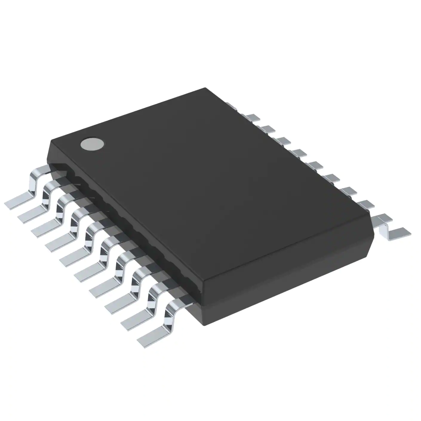
This octal registered transceiver is designed for 1.65-V to 3.6-V VCC operation.
The SN74LVC543ADW contains two sets of D-type latches for temporary storage of data flowing in either direction. Separate latch-enable (LEAB\ or LEBA\) and output-enable (OEAB\ or OEBA\) inputs are provided for each register to permit independent control in either direction of data flow.
The A-to-B enable (CEAB)\ input must be low to enter data from A or to output data from B. If CEAB\ is low and LEAB\ is low, the A-to-B latches are transparent; a subsequent low-to-high transition of LEAB\ places the A latches in the storage mode. With CEAB\ and OEAB\ both low, the 3-state B outputs are active and reflect the data present at the output of the A latches. Data flow for B to A is similar to that of A to B, but uses CEBA\, LEBA\, and OEBA\.
This device is fully specified for partial-power-down applications using Ioff. The Ioff circuitry disables the outputs, preventing damaging current backflow through the device when it is powered down.
To ensure the high-impedance state during power up or power down, OE\ should be tied to VCC through a pullup resistor; the minimum value of the resistor is determined by the current-sinking capability of the driver.
Inputs can be driven from either 3.3-V or 5-V devices. This feature allows the use of these devices as translators in a mixed 3.3-V/5-V system environment.
Feature
- Operates From 1.65 V to 3.6 V
- Inputs Accept Voltages to 5.5 V
- Max tpd of 7 ns at 3.3 V
- Typical VOLP (Output Ground Bounce) <0.8 V at VCC = 3.3 V, TA = 25°C
- Typical VOHV (Output VOH Undershoot) >2 V at VCC = 3.3 V, TA = 25°C
- Supports Mixed-Mode Signal Operation on All Ports (5-V Input/Output Voltage With 3.3-V VCC)
- Ioff Supports Partial-Power-Down Mode Operation
- Latch-Up Performance Exceeds 250 mA Per JESD 17
This octal registered transceiver is designed for 1.65-V to 3.6-V VCC operation.
The SN74LVC543A contains two sets of D-type latches for temporary storage of data flowing in either direction. Separate latch-enable (LEAB\ or LEBA\) and output-enable (OEAB\ or OEBA\) inputs are provided for each register to permit independent control in either direction of data flow.
The A-to-B enable (CEAB)\ input must be low to enter data from A or to output data from B. If CEAB\ is low and LEAB\ is low, the A-to-B latches are transparent; a subsequent low-to-high transition of LEAB\ places the A latches in the storage mode. With CEAB\ and OEAB\ both low, the 3-state B outputs are active and reflect the data present at the output of the A latches. Data flow for B to A is similar to that of A to B, but uses CEBA\, LEBA\, and OEBA\.
This device is fully specified for partial-power-down applications using Ioff. The Ioff circuitry disables the outputs, preventing damaging current backflow through the device when it is powered down.
To ensure the high-impedance state during power up or power down, OE\ should be tied to VCC through a pullup resistor; the minimum value of the resistor is determined by the current-sinking capability of the driver.
Inputs can be driven from either 3.3-V or 5-V devices. This feature allows the use of these devices as translators in a mixed 3.3-V/5-V system environment.


