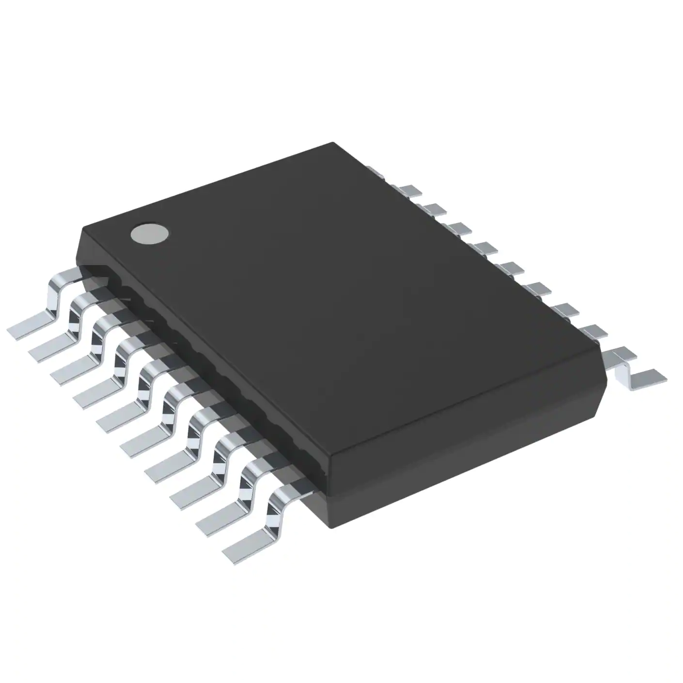
The SN54LVC652A octal bus transceiver and register is designed for 2.7-V to 3.6-V VCC operation, and the SN74LVC652ADW octal bus transceiver and register is designed for 1.65-V to 3.6-V VCC operation.
These devices consist of bus transceiver circuits, D-type flip-flops, and control circuitry arranged for multiplexed transmission of data directly from the data bus or from the internal storage registers.
Output-enable (OEAB and OEBA\) inputs are provided to control the transceiver functions. Select-control (SAB and SBA) inputs are provided to select whether real-time or stored data is transferred. The circuitry used for select control eliminates the typical decoding glitch that occurs in a multiplexer during the transition between stored and real-time data. A low input selects real-time data, and a high input selects stored data. Figure 1 illustrates the four fundamental bus-management functions that are performed with the ’LVC652A devices.
Data on the A or B data bus, or both, is stored in the internal D-type flip-flops by low-to-high transitions at the appropriate clock (CLKAB or CLKBA) inputs, regardless of the select- or enable-control pins. When SAB and SBA are in the real-time transfer mode, it is possible to store data without using the internal D-type flip-flops by simultaneously enabling OEAB and OEBA\. In this configuration, each output reinforces its input. When all other data sources to the two sets of bus lines are at high impedance, each set of bus lines remains at its last state.
Inputs can be driven from either 3.3-V or 5-V devices. This feature allows the use of these devices as translators in a mixed 3.3-V/5-V system environment.
These devices are fully specified for partial-power-down applications using Ioff. The Ioff circuitry disables the outputs, preventing damaging current backflow through the device when it is powered down.
To ensure the high-impedance state during power up or power down, OEBA\ should be tied to VCC through a pullup resistor and OEAB should be tied to GND through a pulldown resistor; the minimum value of the resistor is determined by the current-sinking/current-sourcing capability of the driver.
Feature
- Operate From 1.65 V to 3.6 V
- Inputs Accept Voltages to 5.5 V
- Max tpd of 7.4 ns at 3.3 V
- Typical VOLP (Output Ground Bounce) <0.8 V at VCC = 3.3 V, TA = 25°C
- Typical VOHV (Output VOH Undershoot) >2 V at VCC = 3.3 V, TA = 25°C
- Support Mixed-Mode Signal Operation on All Ports (5-V Input/Output Voltage With 3.3-V VCC)
- Ioff Supports Partial-Power-Down Mode Operation
- ESD Protection Exceeds JESD 22
- 2000-V Human-Body Model (A114-A)
- 200-V Machine Model (A115-A)
- 1000-V Charged-Device Model (C101)
The SN54LVC652A octal bus transceiver and register is designed for 2.7-V to 3.6-V VCC operation, and the SN74LVC652A octal bus transceiver and register is designed for 1.65-V to 3.6-V VCC operation.
These devices consist of bus transceiver circuits, D-type flip-flops, and control circuitry arranged for multiplexed transmission of data directly from the data bus or from the internal storage registers.
Output-enable (OEAB and OEBA\) inputs are provided to control the transceiver functions. Select-control (SAB and SBA) inputs are provided to select whether real-time or stored data is transferred. The circuitry used for select control eliminates the typical decoding glitch that occurs in a multiplexer during the transition between stored and real-time data. A low input selects real-time data, and a high input selects stored data. Figure 1 illustrates the four fundamental bus-management functions that are performed with the ’LVC652A devices.
Data on the A or B data bus, or both, is stored in the internal D-type flip-flops by low-to-high transitions at the appropriate clock (CLKAB or CLKBA) inputs, regardless of the select- or enable-control pins. When SAB and SBA are in the real-time transfer mode, it is possible to store data without using the internal D-type flip-flops by simultaneously enabling OEAB and OEBA\. In this configuration, each output reinforces its input. When all other data sources to the two sets of bus lines are at high impedance, each set of bus lines remains at its last state.
Inputs can be driven from either 3.3-V or 5-V devices. This feature allows the use of these devices as translators in a mixed 3.3-V/5-V system environment.
These devices are fully specified for partial-power-down applications using Ioff. The Ioff circuitry disables the outputs, preventing damaging current backflow through the device when it is powered down.
To ensure the high-impedance state during power up or power down, OEBA\ should be tied to VCC through a pullup resistor and OEAB should be tied to GND through a pulldown resistor; the minimum value of the resistor is determined by the current-sinking/current-sourcing capability of the driver.


