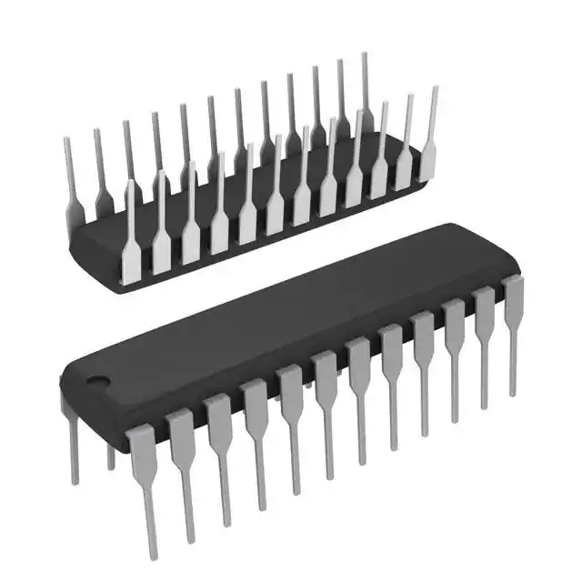
These advanced Schottky devices are capable of performing high-speed arithmetic or logic comparisons on two 8-bit binary or two's complement words. Two fully decoded decisions about words P and Q are externally available at two outputs. These devices are fully expandable to any number of bits without external gates. To compare words of longer lengths, the P > QOUT and P < QOUT outputs of a stage handling less significant bits can be connected to the P > QIN and P < QIN inputs of the next stage handling more significant bits. The cascading paths are implemented with only a two-gate-level delay to reduce overall comparison times for long words. Two alternative methods of cascading are shown in application information.
The latch is transparent when P latch-enable (PLE) input is high; the P-input port is latched
when PLE is low. This provides the designer with temporary storage for the P-data word. The enable circuitry is implemented with minimal delay times to enhance performance when cascaded for longer words. The PLE, P, and Q data inputs utilize pnp input transistors to reduce the low-level current input requirement to typically -0.25 mA, which minimizes dc loading effects.
The SN54AS885 is characterized for operation over the full military temperature range of -55°C to 125°C. The SN74AS885NT is characterized for operation from 0°C to 70°C.
In these cases, P > QOUT follows P > QIN and P < QOUT follows P < QIN.
AG = arithmetically greater than
Feature
- Latchable P-Input Ports With Power-Up Clear
- Choice of Logical or Arithmetic
(Two's Complement) Comparison - Data and PLE Inputs Utilize pnp Input Transistors to Reduce dcLoading Effects
- Approximately 35% Improvement in
ac Performance Over Schottky TTL While Performing More Functions - Cascadable to n Bits While Maintaining High Performance
- 10% Less Power Than STTL for an 8-Bit Comparison
- Package Options Include Plastic Small-Outline (DW) Packages,Ceramic Chip Carriers (FK), and Standard Plastic (NT) and Ceramic(JT) 300-mil DIPs


