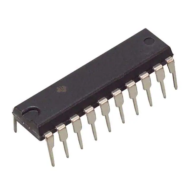
The CD74FCT273E is a positive-edge-triggered, D-type flip-flop with a direct clear (CLR\) input. This device uses a small-geometry BiCMOS technology. The output stage is a combination of bipolar and CMOS transistors that limits the output high level to two diode drops below VCC. This resultant lowering of output swing (0 V to 3.7 V) reduces power-bus ringing [a source of electromagnetic interference (EMI)] and minimizes VCC bounce and ground bounce and their effects during simultaneous output switching. The output configuration also enhances switching speed and is capable of sinking 48 mA.
Information at the data (D) inputs meeting the setup time requirements is transferred to the Q outputs on the positive-going edge of the clock (CLK) pulse. Clock triggering occurs at a particular voltage level and is not directly related to the transition time of the positive-going pulse. When CLK is at either the high or low level, the D input has no effect at the output. All eight flip-flops are controlled by a common clock (CLK) and a common reset (CLR\). The outputs are placed in a low state when CLR\ is taken low, independent of the CLK.
The CD74FCT273E is characterized for operation from 0°C to 70°C.
Feature
- BiCMOS Technology With Low Quiescent Power
- Buffered Inputs
- Direct Clear Input
- 48-mA Output Sink Current
- Output Voltage Swing Limited to 3.7 V
- Controlled Output Edge Rates
- Input/Output Isolation From VCC
- SCR Latch-Up-Resistant BiCMOS Process and Circuit Design
- Applications Include:
- Buffer/Storage Registers
- Shift Registers
- Pattern Generators
- Package Options Include Plastic Small-Outline (M) Package and Standard Plastic (E) DIP
The CD74FCT273 is a positive-edge-triggered, D-type flip-flop with a direct clear (CLR\) input. This device uses a small-geometry BiCMOS technology. The output stage is a combination of bipolar and CMOS transistors that limits the output high level to two diode drops below VCC. This resultant lowering of output swing (0 V to 3.7 V) reduces power-bus ringing [a source of electromagnetic interference (EMI)] and minimizes VCC bounce and ground bounce and their effects during simultaneous output switching. The output configuration also enhances switching speed and is capable of sinking 48 mA.
Information at the data (D) inputs meeting the setup time requirements is transferred to the Q outputs on the positive-going edge of the clock (CLK) pulse. Clock triggering occurs at a particular voltage level and is not directly related to the transition time of the positive-going pulse. When CLK is at either the high or low level, the D input has no effect at the output. All eight flip-flops are controlled by a common clock (CLK) and a common reset (CLR\). The outputs are placed in a low state when CLR\ is taken low, independent of the CLK.
The CD74FCT273 is characterized for operation from 0°C to 70°C.


