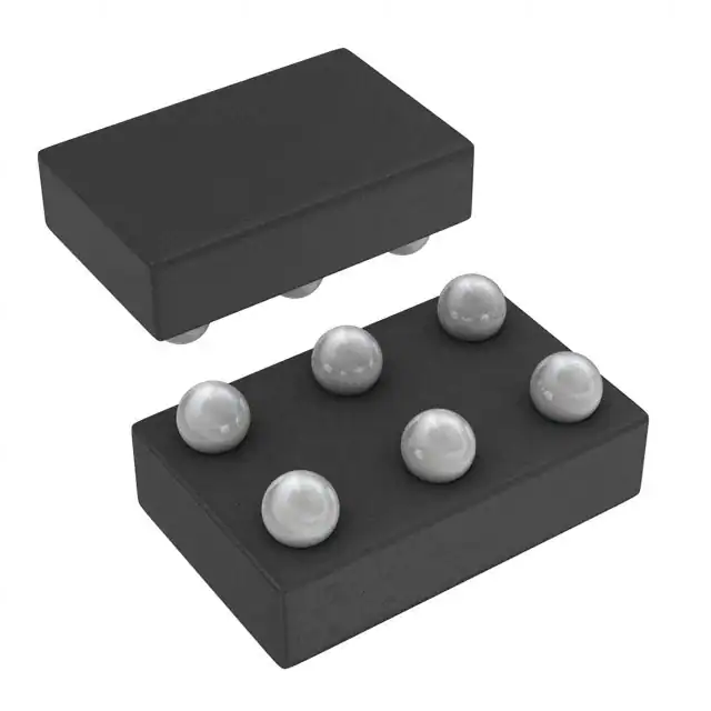
This single D-type latch is designed for 1.65-V to 5.5-V VCC operation.
The SN74LVC1G374YZPR features a 3-state output designed specifically for driving highly capacitive or relatively low-impedance loads. This device is particularly suitable for implementing buffer registers, input/output (I/O) ports, bidirectional bus drivers, and working registers.
NanoStar? and NanoFree? package technology is a major breakthrough in IC packaging concepts, using the die as the package.
On the positive transition of the clock (CLK) input, the Q output is set to the logic level set up at the data (D) input.
A buffered output-enable (OE should be tied to VCC through a pullup resistor; the minimum value of the resistor is determined by the current-sinking capability of the driver.
This device is fully specified for partial-power-down applications using Ioff. The Ioff circuitry disables the outputs, preventing damaging current backflow through the device when it is powered down.
Feature
- Available in the Texas Instruments NanoStar and NanoFree Packages
- Supports 5-V VCC Operation
- Inputs Accept Voltages to 5.5 V
- Provides Down Translation to VCC
- Max tpd of 4 ns at 3.3 V
- Low Power Consumption, 10-μA Max ICC
- ±24-mA Output Drive at 3.3 V
- Ioff Supports Live Insertion, Partial-Power-Down Mode, and Back Drive Protection
- Latch-Up Performance Exceeds 100 mA Per JESD 78, Class II
- ESD Protection Exceeds JESD 22
- 2000-V Human-Body Model (A114-A)
- 200-V Machine Model (A115-A)
- 1000-V Charged-Device Model (C101)
This single D-type latch is designed for 1.65-V to 5.5-V VCC operation.
The SN74LVC1G374 features a 3-state output designed specifically for driving highly capacitive or relatively low-impedance loads. This device is particularly suitable for implementing buffer registers, input/output (I/O) ports, bidirectional bus drivers, and working registers.
NanoStar? and NanoFree? package technology is a major breakthrough in IC packaging concepts, using the die as the package.
On the positive transition of the clock (CLK) input, the Q output is set to the logic level set up at the data (D) input.
A buffered output-enable (OE should be tied to VCC through a pullup resistor; the minimum value of the resistor is determined by the current-sinking capability of the driver.
This device is fully specified for partial-power-down applications using Ioff. The Ioff circuitry disables the outputs, preventing damaging current backflow through the device when it is powered down.


