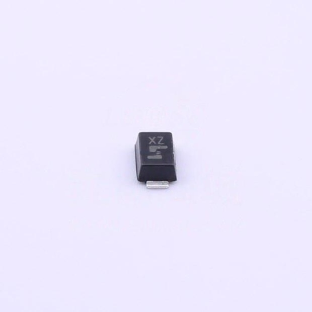
The TPS5120DBT is a dual channel, high-efficiency synchronous buck controller where the outputs run 180 degrees out of phase, which lowers the input current ripple, thereby reducing the input capacitance cost. The PWM/SKIP pin allows the operating mode to switch from PWM mode to skip mode under light load conditions. The skip mode enables a lower operating frequency and shortens the pulse width to the low-side MOSFET, increasing the efficiency under light load conditions. These two modes, along with synchronous-rectifier drivers, dead time, and very low quiescent current, allow power to be conserved and the battery life to be extended under all load conditions. The 1.5 A (typical) high-side and low-side MOSFET drivers on-chip are designed to drive less expensive N-channel MOSFETs. The resistorless current protection and fixed high-side driver voltage simplify the power supply design and reduce the external parts count. Each channel is independent, offering a separate controller, overcurrent protection, and standby control. Sequencing is flexible and can be tailored by choosing different softstart capacitor values. Other features, such as undervoltage lockout, power good, overvoltage, undervoltage, and programmable short-circuit protection promote system reliability.
Feature
- Independent Dual-Outputs Operate 180° Out of Phase
- Wide Input Voltage Range: 4.5-V – 28-V
- Adjustable Output Voltage Down to 0.9 V
- Pin-Selectable PWM/SKIP Mode for High Efficiency Under Light Loads
- Synchronous Buck Operation Allows up to 95% Efficiency
- Separate Standby Control and Overcurrent Protection for Each Channel
- Programmable Short-Circuit Protection
- Low Supply (1 mA) and Shutdown (1 nA) Current
- Power Good Output
- High-Speed Error Amplifiers
- Sequencing Easily Achieved by Selecting Softstart Capacitor Values.
- 5-V Linear Regulator Power Internal IC Circuitry
- 30-Pin TSSOP Packaging
The TPS5120 is a dual channel, high-efficiency synchronous buck controller where the outputs run 180 degrees out of phase, which lowers the input current ripple, thereby reducing the input capacitance cost. The PWM/SKIP pin allows the operating mode to switch from PWM mode to skip mode under light load conditions. The skip mode enables a lower operating frequency and shortens the pulse width to the low-side MOSFET, increasing the efficiency under light load conditions. These two modes, along with synchronous-rectifier drivers, dead time, and very low quiescent current, allow power to be conserved and the battery life to be extended under all load conditions. The 1.5 A (typical) high-side and low-side MOSFET drivers on-chip are designed to drive less expensive N-channel MOSFETs. The resistorless current protection and fixed high-side driver voltage simplify the power supply design and reduce the external parts count. Each channel is independent, offering a separate controller, overcurrent protection, and standby control. Sequencing is flexible and can be tailored by choosing different softstart capacitor values. Other features, such as undervoltage lockout, power good, overvoltage, undervoltage, and programmable short-circuit protection promote system reliability.


