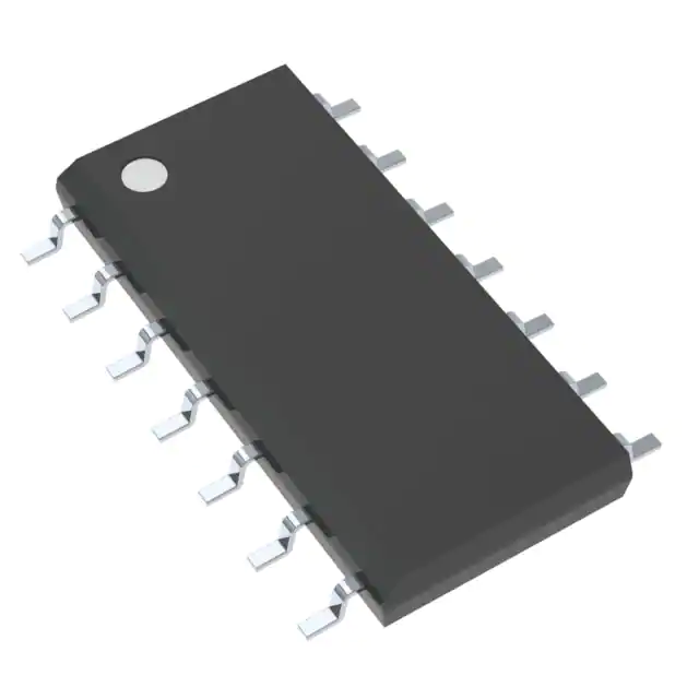
The ’HCT74 devices contain two independent D-type positive-edge-triggered flip-flops. A low level at the preset (PRE)\ or clear (CLR)\ inputs sets or resets the outputs, regardless of the levels of the other inputs. When PRE\ and CLR\ are inactive (high), data at the data (D) input meeting the setup time requirements are transferred to the outputs on the positive-going edge of the clock (CLK) pulse. Clock triggering occurs at a voltage level and is not directly related to the rise time of CLK. Following the hold-time interval, data at the D input may be changed without affecting the levels at the outputs.
Feature
- Operating Voltage Range of 4.5 V to 5.5 V
- Outputs Can Drive Up To 10 LSTTL Loads
- Low Power Consumption, 40-μA Max ICC
- Typical tpd = 17 ns
- ±4-mA Output Drive at 5 V
- Low Input Current of 1 μA Max
- Inputs Are TTL-Voltage Compatible
The ’HCT74 devices contain two independent D-type positive-edge-triggered flip-flops. A low level at the preset (PRE)\ or clear (CLR)\ inputs sets or resets the outputs, regardless of the levels of the other inputs. When PRE\ and CLR\ are inactive (high), data at the data (D) input meeting the setup time requirements are transferred to the outputs on the positive-going edge of the clock (CLK) pulse. Clock triggering occurs at a voltage level and is not directly related to the rise time of CLK. Following the hold-time interval, data at the D input may be changed without affecting the levels at the outputs.


