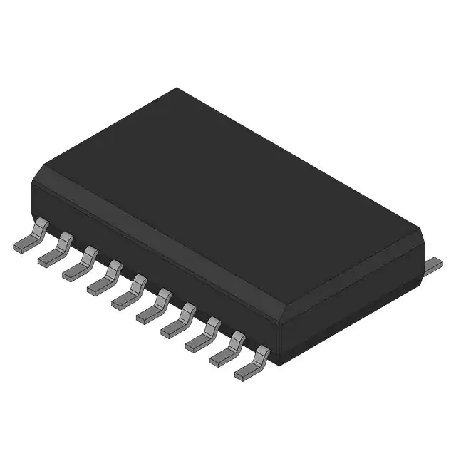
General description
The 74LVC273 has eight edge-triggered, D-type flip-flops with individual Dn inputs and Qn outputs. The common clock (CP) and master reset (MR) inputs load and reset (clear) all flip-flops simultaneously. The state of each Dn input, one set-up time before the LOW-to-HIGH clock transition, is transferred to the corresponding output (Qn) of the flip-flop. All outputs will be forced LOW independently of clock or data inputs by a LOW voltage level on the MR input.
The device is useful for applications where the true output only is required and the clock and master reset are common to all storage elements.
Features and benefits
Wide supply voltage range from 1.2 V to 3.6 V
Inputs accept voltages up to 5.5 V
CMOS low power consumption
Direct interface with TTL levels
Output drive capability 50
transmission lines at +85°C
Complies with JEDEC standard:
JESD8-7A (1.65 V to 1.95 V)
JESD8-5A (2.3 V to 2.7 V)
JESD8-C/JESD36 (2.7 V to 3.6 V)
ESD protection:
HBM JESD22-A114F exceeds 2000 V
MM JESD22-A115-B exceeds 200 V
CDM JESD22-C101E exceeds 1000 V
Specified from -40℃ to +85℃ and 40℃ to +125℃.
(Picture:Pinout / Diagram)


