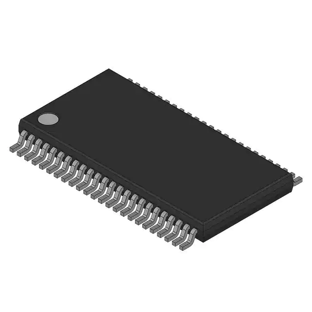
This 16-bit edge-triggered D-type flip-flop is designed for 2.7-V to 3.6-V VCC operation.
The SN74LVC16374DGG is particularly suitable for implementing buffer registers, I/O ports, bidirectional bus drivers, and working registers. It can be used as two 8-bit flip-flops or one 16-bit flip-flop. On the positive transition of the clock (CLK) input, the Q outputs of the flip-flop take on the logic levels set up at the data (D) inputs.
A buffered output-enable (OE\) input can be used to place the eight outputs in either a normal logic state (high or low logic levels) or a high-impedance state. In the high-impedance state, the outputs neither load nor drive the bus lines significantly. The high-impedance state and the increased drive provide the capability to drive bus lines without need for interface or pullup components.
OE\ does not affect internal operations of the flip-flop. Old data can be retained or new data can be entered while the outputs are in the high-impedance state.
To ensure the high-impedance state during power up or power down, OE\ should be tied to VCC through a pullup resistor; the minimum value of the resistor is determined by the current-sinking capability of the driver.
Active bus-hold circuitry is provided to hold unused or floating data inputs at a valid logic level.
The SN74LVC16374DGG is characterized for operation from -40°C to 85°C.
Feature
- Member of the Texas InstrumentsWidebusTM Family
- EPICTM (Enhanced-Performance Implanted CMOS) Submicron Process
- Typical VOLP (Output Ground Bounce)
< 0.8 V at VCC = 3.3 V, TA = 25°C - Typical VOHV (Output VOH Undershoot)
> 2 V at VCC = 3.3 V, TA = 25°C - Latch-Up Performance Exceeds 250 mA
Per JEDEC Standard JESD-17 - Bus Hold on Data Inputs Eliminates the Need for External Pullup/Pulldown Resistors
- Package Options Include Plastic 300-mil Shrink Small-Outline (DL) and Thin Shrink Small-Outline (DGG) Packages


