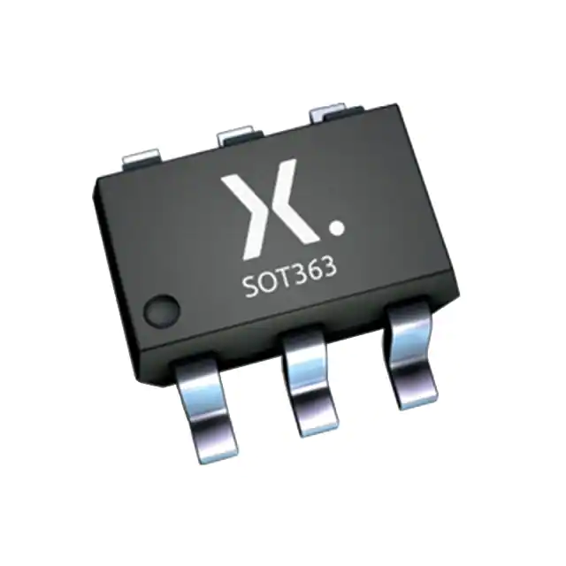
The 74LVC1G175GW is a single positive-edge triggered D-type Flip-flop with individual data (D) input, clock input, master reset (MR) input and Q output. The master reset (MR) is an asynchronous active low input and operates independently of the clock input. Information on the data input is transferred to the Q output on the low-to-high transition of the clock pulse. The D input must be stable one set-up time prior to the low-to-high clock transition for predictable operation. The inputs can be driven from either 3.3 or 5V devices. This feature allows the use of this device in a mixed 3.3 and 5V environment. This device is fully specified for partial power-down applications using IOFF. The IOFF circuitry disables the output, preventing the damaging backflow current through the device when it is powered down. Schmitt trigger action at all inputs makes the circuit highly tolerant of slower input rise and fall times.
Feature
- High noise immunity
- CMOS low power consumption
- Latch-up performance exceeds 250mA
- Direct interface with TTL levels
- ±24mA Output drive current

