EPIC-IIB is a trademark of Texas Instruments Incorporated.
DescriptionThese 9-bit flip-flops feature 3-state outputs designed specifically for driving highly capacitive or relatively low-impedance loads. They are particularly suitable for implementing wider buffer registers, I/O ports, bidirectional bus drivers with parity, and working registers.
With the clock-enable (CLKEN\) input low, the nine D-type edge-triggered flip-flops enter data on the low-to-high transitions of the clock. Taking CLKEN\ high disables the clock buffer, thus latching the outputs. Taking the clear (CLR\) input low causes the nine Q outputs to go low, independently of the clock.
A buffered output-enable (OE\) input can be used to place the nine outputs in either a normal logic state (high or low logic level) or a high-impedance state. In the high-impedance state, the outputs neither load nor drive the bus lines significantly. The high-impedance state and increased drive provide the capability to drive bus lines without need for interface or pullup components.
When VCC is between 0 and 2.1 V, the device is in the high-impedance state during power up or power down. However, to ensure the high-impedance state above 2.1 V, OE\ should be tied to VCC through a pullup resistor; the minimum value of the resistor is determined by the current-sinking capability of the driver.
The SN54ABT823 is characterized for operation over the full military temperature range of -55°C to 125°C. The SN74ABT823DBR is characterized for operation from -40°C to 85°C.
Feature
- State-of-the-ArtEPIC-II BTM BiCMOS Design Significantly Reduces Power Dissipation
- ESD Protection Exceeds 2000 V Per MIL-STD-883, Method 3015; Exceeds 200 V Using Machine Model (C = 200 pF, R = 0)
- Latch-Up Performance Exceeds 500 mA Per JEDEC Standard JESD-17
- Typical VOLP (Output Ground Bounce) < 1 V at VCC = 5 V, TA = 25°C
- High-Impedance State During Power Up and Power Down
- High-Drive Outputs (-32-mA IOH, 64-mA IOL)
- Buffered Control Inputs to Reduce dc Loading Effects
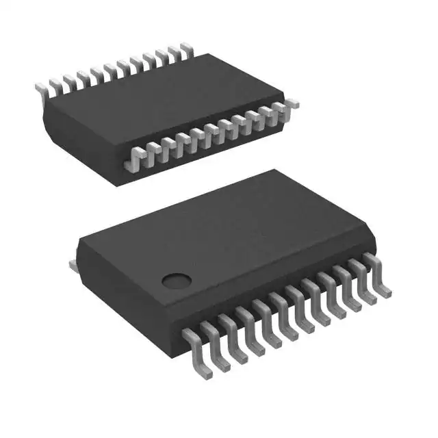
- Package Options Include Plastic Small-Outline (DW) and Shrink Small-Outline (DB) Packages, Ceramic Chip Carriers (FK) and Flatpacks (W), and Standard Plastic (NT) and Ceramic (JT) DIPs
EPIC-IIB is a trademark of Texas Instruments Incorporated.
DescriptionThese 9-bit flip-flops feature 3-state outputs designed specifically for driving highly capacitive or relatively low-impedance loads. They are particularly suitable for implementing wider buffer registers, I/O ports, bidirectional bus drivers with parity, and working registers.
With the clock-enable (CLKEN\) input low, the nine D-type edge-triggered flip-flops enter data on the low-to-high transitions of the clock. Taking CLKEN\ high disables the clock buffer, thus latching the outputs. Taking the clear (CLR\) input low causes the nine Q outputs to go low, independently of the clock.
A buffered output-enable (OE\) input can be used to place the nine outputs in either a normal logic state (high or low logic level) or a high-impedance state. In the high-impedance state, the outputs neither load nor drive the bus lines significantly. The high-impedance state and increased drive provide the capability to drive bus lines without need for interface or pullup components.
When VCC is between 0 and 2.1 V, the device is in the high-impedance state during power up or power down. However, to ensure the high-impedance state above 2.1 V, OE\ should be tied to VCC through a pullup resistor; the minimum value of the resistor is determined by the current-sinking capability of the driver.
The SN54ABT823 is characterized for operation over the full military temperature range of -55°C to 125°C. The SN74ABT823 is characterized for operation from -40°C to 85°C.


