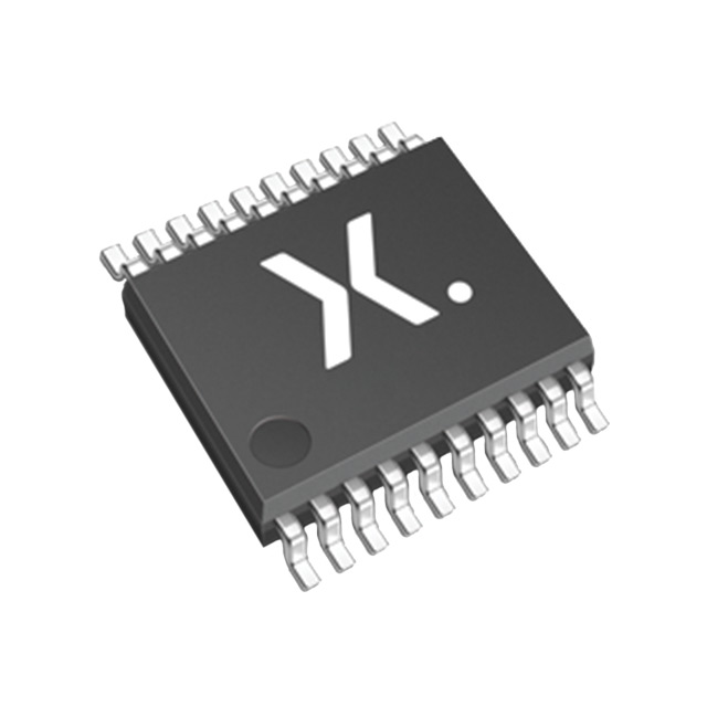
DESCRIPTION:
The 74LVC273 is a low-voltage Si-gate CMOS device, superior to most advanced CMOS compatible TTL families. The 74LVC273 has eight edge-triggered , D-type flip-flops with individual D inputs and Q outputs. The common clock (CP) and master reset (MR) inputs load and reset (clear) all flip-flops simultaneously. The state of each D input, one set-up time before the LOW-to-HIGH clock transition, is transferred to the corresponding output (Qn) of the flip-flop. All outputs will be forced LOW independently of clock or data inputs by a LOW voltage level on the MR input. The device is useful for applications where the true output only is required and the clock and master reset are common to all storage elements.
FEATURES:
• Wide supply voltage range of 1.2V to 3.6V
• Conforms to JEDEC standard 8-1A
• Inputs accept voltages up to 5.5V
• CMOS low power consumption
• Direct interface with TTL levels
• Output drive capability 50W transmission lines @ 85°C
(Picture:Pinout / Diagram)


