CD4086BMT contains one 4-wide 2-input AND-OR-INVERT gate with an INHIBIT/(EXP\) input and an ENABLE/EXP input. For a4-wide A-O-I function INHIBIT/(EXP\) is tied to VSS and ENABLE/EXP to VDD. See Fig. 10 and its associatedexplanation for applications where a capability greater than 4-wide is required.
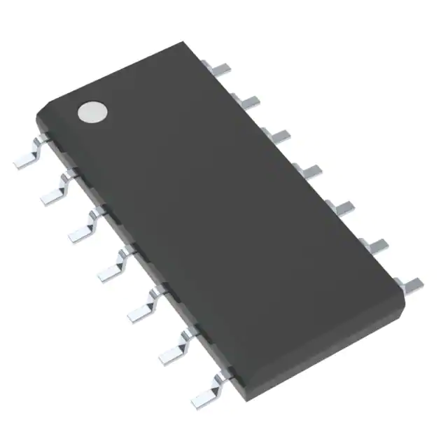
The CD4086BMT types are supplied in 14-lead hermetic dual-in-line ceramic packages (F3A suffix), 14-lead dual-in-line plastic packages (E suffix), 14-lead small-outline packages (M, MT, M96, and NSR suffixes), and 14-lead thin shrink small-outline packages (PW and PWR suffixes).
Feature
- Medium-speed operation - tPHL = 90 ns; tPLH = 140 ns (typ.) at 10 V
- INHIBIT and ENABLE inputs
- Buffered outputs
- 100% tested for quiescent current at 20 V
- Maximum input leakage current of 18 V over full package-temperature range; 100 nA at 18 V and 25°C
- Noise margin (over full package temperature range): 1 V at VDD = 5 V 2 V at VDD = 10 V 2.5 V at VDD = 15 V
- Standardized, symmetrical output characteristics
- 5-V, 10-V, and 15-V parametric ratings
- Meets all requirements of JEDEC Tentative Standard No. 13B, "Standard Specifications for Description of 'B' Series CMOS Devices"
CD4086B contains one 4-wide 2-input AND-OR-INVERT gate with an INHIBIT/(EXP\) input and an ENABLE/EXP input. For a4-wide A-O-I function INHIBIT/(EXP\) is tied to VSS and ENABLE/EXP to VDD. See Fig. 10 and its associatedexplanation for applications where a capability greater than 4-wide is required.
The CD4086B types are supplied in 14-lead hermetic dual-in-line ceramic packages (F3A suffix), 14-lead dual-in-line plastic packages (E suffix), 14-lead small-outline packages (M, MT, M96, and NSR suffixes), and 14-lead thin shrink small-outline packages (PW and PWR suffixes).


