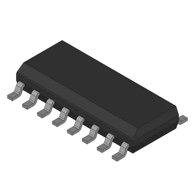
The 74HC40105D is a 4-bit x 16-word FIFO Register can handle input and output data at different shifting rates. This feature makes it particularly useful as a buffer between asynchronous systems. Each word position in the register is clocked by a control flip-flop, which stores a marker bit. A logic 1 signifies that the data at that position is filled and a logic 0 denotes a vacancy in that position. The control flip-flop detects the state of the preceding flip-flop and communicates its own status to the succeeding flip-flop. When a control flip-flop is in the logic 0 state and sees a logic 1 in the preceding flip-flop, it generates a clock pulse. The clock pulse transfers data from the preceding four data latches into its own four data latches and resets the preceding flip-flop to logic 0. The first and last control flip-flops have buffered outputs. All empty locations 'bubble' automatically to the input end and all valid data ripples through to the output end.
Feature
- Independent asynchronous inputs and outputs
- Expandable in either direction
- Reset capability
- Status indicators on inputs and outputs
- 3-state Outputs
- CMOS Input levels
