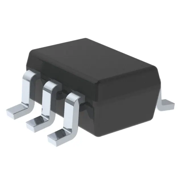
This dual inverter buffer and driver is designed for 1.65-V to 5.5-V VCC operation.
The output of the SN74LVC2G06DCKR device is an open-drain which can be connected to other open-drain outputs to implement active-low, wired-OR, or active-high wired-AND functions. The maximum sink current is 32 mA.
This device is fully specified for partial-power-down applications using Ioff. The Ioff circuitry disables the outputs, preventing damaging current backflow through the device when it is powered down.
NanoFree? package technology is a major breakthrough in IC packaging concepts, using the die as the package.
Feature
- IOFF Supports live insertion, partial-power-down mode and back-drive protection
- Supports down-translation
- Inputs and open-drain outputs accept voltages up to 5.5V
- Latch-up performance exceeds 250mA per JESD 17
- 3.4ns at 3.3V Propagation delay (tpd)
- 10µA ICC Low power consumption
- ±24mA Output drive at 3.3 V
- <0.8V at VCC = 3.3V, TA = 25°C VOLP (output ground bounce)
- >2V at VCC = 3.3V, TA = 25°C VOHV (output VOH undershoot)
- Green product and no Sb/Br


