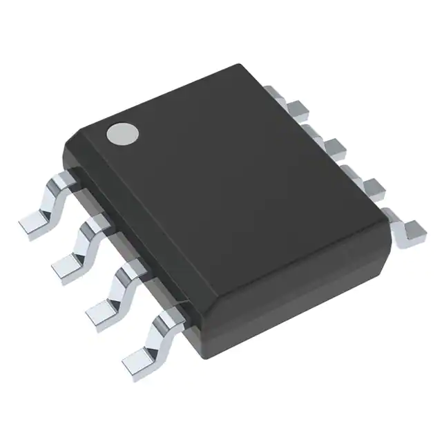
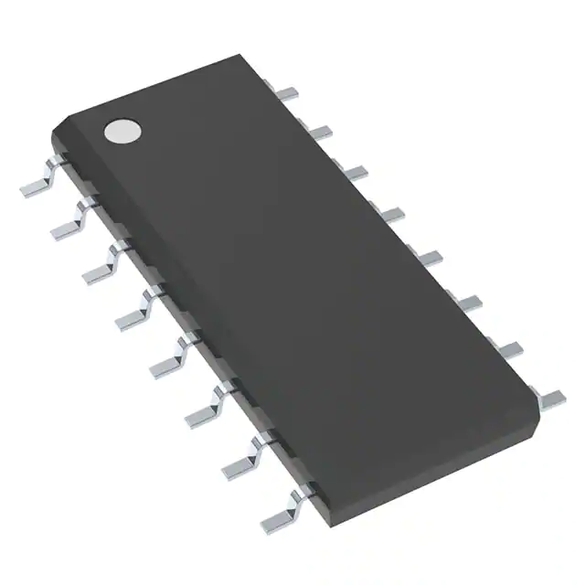
The TL5001CDR and TL5001A incorporate on a single monolithic chip all the functions required for a pulse-width-modulation (PWM) control circuit. Designed primarily for power-supply control, the TL5001/A contains an error amplifier, a regulator, an oscillator, a PWM comparator with a dead-time-control input, undervoltage lockout (UVLO), short-circuit protection (SCP), and an open-collector output transistor. The TL5001A has a typical reference voltage tolerance of ±3% compared to ±5% for the TL5001.
The error-amplifier common-mode voltage ranges from 0 V to 1.5 V. The noninverting input of the error amplifier is connected to a 1-V reference. Dead-time control (DTC) can be set to provide 0% to 100% dead time by connecting an external resistor between DTC and GND. The oscillator frequency is set by terminating RT with an external resistor to GND. During low VCC conditions, the UVLO circuit turns the output off until VCC recovers to its normal operating range.
The TL5001C and TL5001AC are characterized for operation from –20°C to 85°C. The TL5001I and TL5001AI are characterized for operation from –40°C to 85°C. The TL5001Q and TL5001AQ are characterized for operation from–40°C to 125°C. The TL5001M and TL5001AM are characterized for operation from –55°C to 125°C.
Feature
- Complete PWM Power Control
- 3.6-V to 40-V Operation
- Internal Undervoltage-Lockout Circuit
- Internal Short-Circuit Protection
- Oscillator Frequency . . . 20 kHz to 500 kHz
- Variable Dead Time Provides Control Over Total Range
- ±3% Tolerance on Reference Voltage (TL5001A)
- Available in Q-Temp Automotive HighRel Automotive Applications Configuration Control / Print Support Qualification to Automotive Standards
The TL5001 and TL5001A incorporate on a single monolithic chip all the functions required for a pulse-width-modulation (PWM) control circuit. Designed primarily for power-supply control, the TL5001/A contains an error amplifier, a regulator, an oscillator, a PWM comparator with a dead-time-control input, undervoltage lockout (UVLO), short-circuit protection (SCP), and an open-collector output transistor. The TL5001A has a typical reference voltage tolerance of ±3% compared to ±5% for the TL5001.
The error-amplifier common-mode voltage ranges from 0 V to 1.5 V. The noninverting input of the error amplifier is connected to a 1-V reference. Dead-time control (DTC) can be set to provide 0% to 100% dead time by connecting an external resistor between DTC and GND. The oscillator frequency is set by terminating RT with an external resistor to GND. During low VCC conditions, the UVLO circuit turns the output off until VCC recovers to its normal operating range.
The TL5001C and TL5001AC are characterized for operation from –20°C to 85°C. The TL5001I and TL5001AI are characterized for operation from –40°C to 85°C. The TL5001Q and TL5001AQ are characterized for operation from–40°C to 125°C. The TL5001M and TL5001AM are characterized for operation from –55°C to 125°C.


