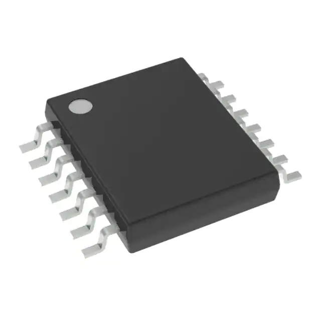
The SNx4LVC74A devices integrate two positive-edge triggered D-type flip-flops in one convenient device.
The SN54LVC74A is designed for 2.7-V to 3.6-V VCC operation, and the SN74LVC74APWRG4 is designed for 1.65-V to 3.6-V VCC operation.
A low level at the preset (CLR are inactive (high), data at the data (D) input meeting the setup time requirements is transferred to the outputs on the positive-going edge of the clock pulse. Clock triggering occurs at a voltage level and is not directly related to the rise time of the clock pulse. Following the hold-time interval, data at the D input can be changed without affecting the levels at the outputs.
The data I/Os and control inputs are overvoltage tolerant. This feature allows the use of these devices for down-translation in a mixed-voltage environment.
Feature
- Operate From 1.65 V to 3.6 V
- Inputs Accept Voltages to 5.5 V
- Maximum tpd of 5.2 ns at 3.3 V
- Typical VOLP (Output Ground Bounce) <0.8 V at VCC = 3.3 V, TA = 25°C
- Typical VOHV (Output VOH Undershoot) >2 V at VCC = 3.3 V, TA = 25°C
- Latch-Up Performance Exceeds 250 mA Per JESD 17
- ESD Protection Exceeds JESD 22
- 2000-V Human-Body Model (A114-A)
- 1000-V Charged-Device Model (C101)
The SNx4LVC74A devices integrate two positive-edge triggered D-type flip-flops in one convenient device.
The SN54LVC74A is designed for 2.7-V to 3.6-V VCC operation, and the SN74LVC74A is designed for 1.65-V to 3.6-V VCC operation.
A low level at the preset (CLR are inactive (high), data at the data (D) input meeting the setup time requirements is transferred to the outputs on the positive-going edge of the clock pulse. Clock triggering occurs at a voltage level and is not directly related to the rise time of the clock pulse. Following the hold-time interval, data at the D input can be changed without affecting the levels at the outputs.
The data I/Os and control inputs are overvoltage tolerant. This feature allows the use of these devices for down-translation in a mixed-voltage environment.


