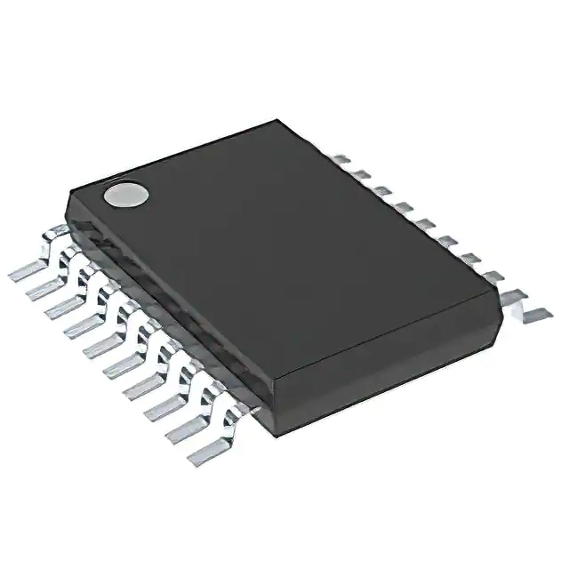
These 8-bit flip-flops with 3-state outputs are designed specifically for driving highly capacitive or relatively low-impedance loads. They are particularly suitable for implementing buffer registers, I/O ports, bidirectional bus drivers, and working registers.
The eight flip-flops are edge-triggered D-type flip-flops. On the positive transition of the clock (CLK), the Q\ outputs are set to the complement of the logic levels set up at the data (D) inputs.
A buffered output-enable () input can be used to place the eight outputs in either a normal logic state (high or low logic levels) or a high-impedance state. In the high-impedance state, the outputs neither load nor drive the bus lines significantly. The high-impedance state and increased drive provide the capability to drive bus lines without need for interface or pullup components.
does not affect the internal operations of the flip-flop. Previously stored data can be retained or new data can be entered while the outputs are in the high-impedance state.
To ensure the high-impedance state during power up or power down, should be tied to VCC through a pullup resistor; the minimum value of the resistor is determined by the current-sinking capability of the driver.
The SN54ABT534 is characterized for operation over the full military temperature range of -55°C to 125°C. The SN74ABT534APWRG4 is characterized for operation from -40°C to 85°C.
Feature
- State-of-the-Art EPIC-IIBTM BiCMOS Design Significantly Reduces Power Dissipation
- Latch-Up Performance Exceeds 500 mA Per JEDEC Standard JESD-17
- Typical VOLP (Output Ground Bounce) < 1 V at VCC = 5 V, TA = 25°C
- High-Drive Outputs (-32-mA IOH, 64-mA IOL)
- ESD Protection Exceeds 2000 V Per MIL-STD-883, Method 3015; Exceeds 200 V Using Machine Model (C = 200 pF, R = 0)
- Package Options Include Plastic Small-Outline (DW), Shrink Small-Outline (DB), and Thin Shrink Small-Outline (PW) Packages, Ceramic Chip Carriers (FK), Plastic (N) and Ceramic (J) DIPs, and Ceramic Flat (W) Package


