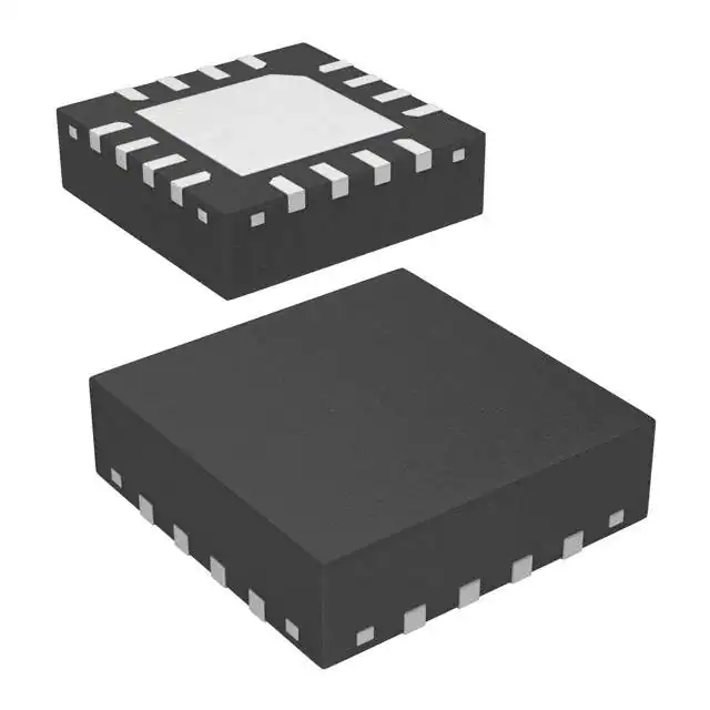
The HMC745LC3 is a XOR/XNOR gate function designed to support data transmission rates of up to 13 Gbps, and clock frequencies as high as 13 GHz. The HMC745LC3 also features an output level control pin, VR, which permits loss compensation or signal level optimization.
All input and output signals to the HMC745LC3 are terminated with 50 Ω to VCC on-chip, and can be either ac-coupled or dc-coupled
Inputs or outputs can be connected directly to a 50 Ω VCC terminated system, while dc blocking capacitors may be used if the terminating system is 50 Ω to ground. The HMC745LC3 operates from a single 3.3 V dc supply, and is available in a ceramic, RoHS compliant, 3 mm × 3 mm LCC package.
Feature
- Inputs terminated internally at 50 Ω
- Differential and single-ended operation
- Fast rise and fall times: 21/19 ps
- Low power consumption: 240 mW (typical)
- Programmable DifferentialOutput voltage swing: 600 mV to 1200 mV
- Propagation delay: 95 ps
- Single supply: 3.3 V
- 16-terminal, ceramic 3 mm × 3 mm LCC package
Applications
- RF automatic test equipment (ATE) applications
- Broadband test and measurement
- Serial data transmission up to 13 Gbps
- Digital logic systems up to 13 GHz
(Picture: Pinout)


