Widebus is a trademark of Texas Instruments Incorporated.
DescriptionThe 'ALVTH16821 devices are 20-bit bus-interface flip-flops with 3-state outputs designed for 2.5-V or 3.3-V VCC operation, but with the capability to provide a TTL interface to a 5-V system environment.
The devices can be used as two 10-bit flip-flops or one 20-bit flip-flop. The 20-bit flip-flops are edge-triggered D-type flip-flops. On the positive transition of the clock (CLK), the flip-flops store the logic levels set up at the D inputs.
A buffered output-enable (OE\) input can be used to place the ten outputs in either a normal logic state (high or low level) or a high-impedance state. In the high-impedance state, the outputs neither load nor drive the bus lines significantly. The high-impedance state and increased drive provide the capability to drive bus lines without need for interface or pullup components.
OE\ does not affect the internal operation of the flip-flops. Old data can be retained or new data can be entered while the outputs are in the high-impedance state.
When VCC is between 0 and 1.2 V, the device is in the high-impedance state during power up or power down. However, to ensure the high-impedance state above 1.2 V, OE\ should be tied to VCC through a pullup resistor; the minimum value of the resistor is determined by the current-sinking capability of the driver.
Active bus-hold circuitry is provided to hold unused or floating data inputs at a valid logic level.
The SN54ALVTH16821 is characterized for operation over the full military temperature range of -55°C to 125°C. The SN74ALVTH16821VR is characterized for operation from -40°C to 85°C.
Feature
- State-of-the-Art Advanced BiCMOS Technology (ABT)WidebusTM Design for 2.5-V and 3.3-V Operation and Low Static Power Dissipation
- Support Mixed-Mode Signal Operation (5-V Input and Output Voltages With 2.3-V to 3.6-V VCC)
- Typical VOLP (Output Ground Bounce) < 0.8 V at VCC = 3.3 V, TA = 25°C
- High-Drive (-24/24 mA at 2.5-V and-32/64 mA at 3.3-V VCC)
- Power Off Disables Outputs, Permitting Live Insertion
- High-Impedance State During Power Up and Power Down Prevents Driver Conflict
- Uses Bus Hold on Data Inputs in Place of External Pullup/Pulldown Resistors to Prevent the Bus From Floating
- Auto3-State Eliminates Bus Current Loading When Output Exceeds VCC + 0.5 V
- Latch-Up Performance Exceeds 250 mA Per JESD 17
- ESD Protection Exceeds 2000 V Per MIL-STD-883, Method 3015; Exceeds 200 V Using Machine Model; and Exceeds 1000 V Using Charged-Device Model, Robotic Method
- Flow-Through Architecture Facilitates Printed Circuit Board Layout
- Distributed VCC and GND Pin Configuration Minimizes High-Speed Switching Noise
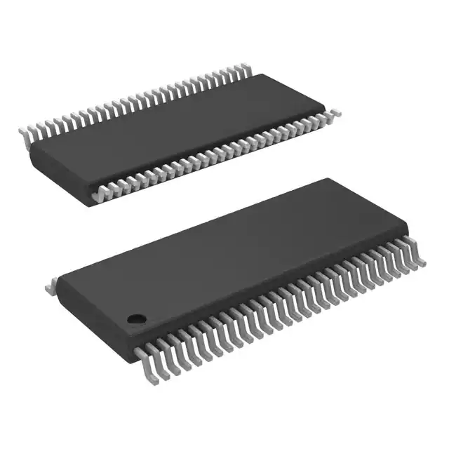
- Package Options Include Plastic Shrink Small-Outline (DL), Thin Shrink Small-Outline (DGG), Thin Very Small-Outline (DGV) Packages, and 380-mil Fine-Pitch Ceramic Flat (WD) Package
Widebus is a trademark of Texas Instruments Incorporated.
The 'ALVTH16821 devices are 20-bit bus-interface flip-flops with 3-state outputs designed for 2.5-V or 3.3-V VCC operation, but with the capability to provide a TTL interface to a 5-V system environment.
The devices can be used as two 10-bit flip-flops or one 20-bit flip-flop. The 20-bit flip-flops are edge-triggered D-type flip-flops. On the positive transition of the clock (CLK), the flip-flops store the logic levels set up at the D inputs.
A buffered output-enable (OE\) input can be used to place the ten outputs in either a normal logic state (high or low level) or a high-impedance state. In the high-impedance state, the outputs neither load nor drive the bus lines significantly. The high-impedance state and increased drive provide the capability to drive bus lines without need for interface or pullup components.
OE\ does not affect the internal operation of the flip-flops. Old data can be retained or new data can be entered while the outputs are in the high-impedance state.
When VCC is between 0 and 1.2 V, the device is in the high-impedance state during power up or power down. However, to ensure the high-impedance state above 1.2 V, OE\ should be tied to VCC through a pullup resistor; the minimum value of the resistor is determined by the current-sinking capability of the driver.
Active bus-hold circuitry is provided to hold unused or floating data inputs at a valid logic level.
The SN54ALVTH16821 is characterized for operation over the full military temperature range of -55°C to 125°C. The SN74ALVTH16821 is characterized for operation from -40°C to 85°C.


