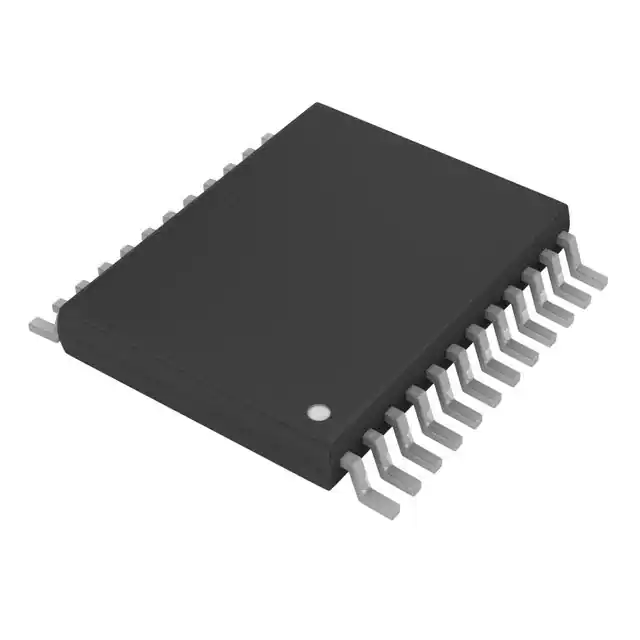
The SN74LV8151DGVR is a 10-bit universal Schmitt-trigger buffer with 3-state outputs, designed for 2-V to 5.5-V VCC operation. The logic control (T/C\) pin allows the user to configure Y1 to Y8 as noninverting or inverting outputs. When T/C\ is high, the Y outputs are noninverted (true logic ), and when T/C\ is low, the Y outputs are inverted (complementary logic).
When output-enable (OE)\ input is low, the device passes data from Dn to Yn. When OE\ is high, the Y outputs are in the high-impedance state. The path A to P is a simple Schmitt-trigger buffer, and the path B to N is a simple Schmitt-trigger inverter.
This device is fully specified for partial-power-down applications using Ioff. The Ioff circuitry disables the outputs, preventing damaging current backflow through the device when it is powered down.
To ensure the high-impedance state during power up or power down, OE\ should be tied to VCC through a pullup resistor; the minimum value of the resistor is determined by the current-sinking capability of the driver.
Feature
- 2-V to 5.5-V VCC Operation
- Max tpd of 15 ns at 5 V
- Schmitt-Trigger Inputs Allow for Slow Input Rise/Fall Time
- Polarity Control for Y Outputs Selects True or Complementary Logic
- Typical VOLP (Output Ground Bounce) <0.8 V at VCC = 3.3 V, TA = 25°C
- Typical VOHV (Output VOH Undershoot) >>2.3 V at VCC = 3.3 V, TA = 25°C
- Ioff Supports Partial-Power-Down Mode Operation
- Supports Mixed-Mode Voltage Operation on All Ports
- Latch-Up Performance Exceeds 250 mA Per JESD 17
- ESD Protection Exceeds JESD 22
- 2000-V Human-Body Model (A114-A)
- 200-V Machine Model (A115-A)
- 1000-V Charged-Device Model (C101)
The SN74LV8151 is a 10-bit universal Schmitt-trigger buffer with 3-state outputs, designed for 2-V to 5.5-V VCC operation. The logic control (T/C\) pin allows the user to configure Y1 to Y8 as noninverting or inverting outputs. When T/C\ is high, the Y outputs are noninverted (true logic ), and when T/C\ is low, the Y outputs are inverted (complementary logic).
When output-enable (OE)\ input is low, the device passes data from Dn to Yn. When OE\ is high, the Y outputs are in the high-impedance state. The path A to P is a simple Schmitt-trigger buffer, and the path B to N is a simple Schmitt-trigger inverter.
This device is fully specified for partial-power-down applications using Ioff. The Ioff circuitry disables the outputs, preventing damaging current backflow through the device when it is powered down.
To ensure the high-impedance state during power up or power down, OE\ should be tied to VCC through a pullup resistor; the minimum value of the resistor is determined by the current-sinking capability of the driver.


