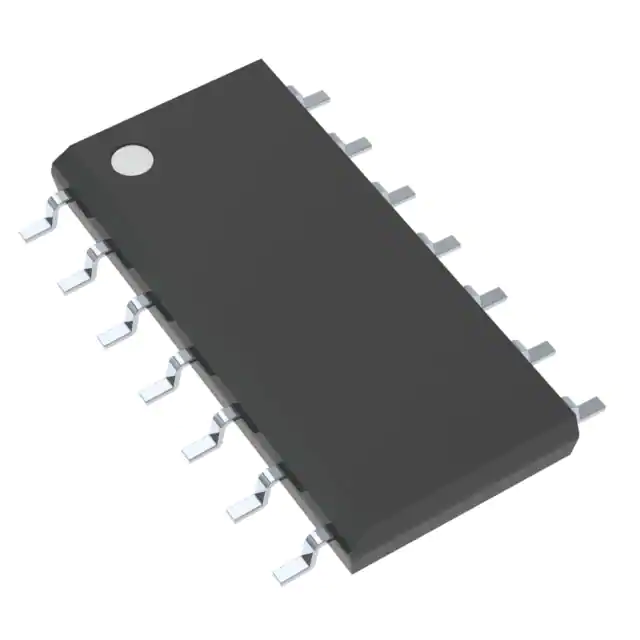
The CD4093BQM96Q1 consists of four Schmitt-trigger circuits. Each circuit functions as a two-input NAND gate, with Schmitt-trigger action on both inputs. The gate switches at different points for positive- and negative-going signals. The difference between the positive voltage (VP) and the negative voltage (VN) is defined as hysteresis voltage (VH)(see Figure 2).
The CD4093BQM96Q1 is available in 14-lead small-outline plastic package (M96) and 14-lead thin shrink small-outline packages (PWR suffixes).
Feature
- Qualified for Automotive Applications
- Schmitt-Trigger Action on Each Input With No External Components
- Hysteresis Voltage Typically 0.9 V at VDD = 5 V and 2.3 V at VDD = 10 V
- Noise Immunity Greater Than 50%
- No Limit on Input Rise and Fall Times
- Standardized, Symmetrical Output Characteristics
- 100% Tested for Quiescent Current at 20 V
- Maximum Input Current of 1μA at 18 V Over Full Package Temperature Range, 100 nA at 18 V and 25°C
- 5-V, 10-V, and 15-V Parametric Ratings
- ESD Protection Level Per AEC-Q100 Classification
- 2000-V (H2) Human-Body Model
- 200-V (M3) Machine-Model
- 1000-V (C5) Charge-Device Model
- Applications
- Wave and Pulse Shapers
- High-Noise-Environment Systems
- Monostable Multivibrators
- Astable Multivibrators
- NAND Logic
The CD4093B-Q1 consists of four Schmitt-trigger circuits. Each circuit functions as a two-input NAND gate, with Schmitt-trigger action on both inputs. The gate switches at different points for positive- and negative-going signals. The difference between the positive voltage (VP) and the negative voltage (VN) is defined as hysteresis voltage (VH)(see Figure 2).
The CD4093B-Q1 is available in 14-lead small-outline plastic package (M96) and 14-lead thin shrink small-outline packages (PWR suffixes).


