CD4085 contains a pair of AND-OR-INVERT gates, each consisting of two 2-input AND gates driving a 3-input NOR gate. Individual inhibit controls are provided for both A-O-I gates.
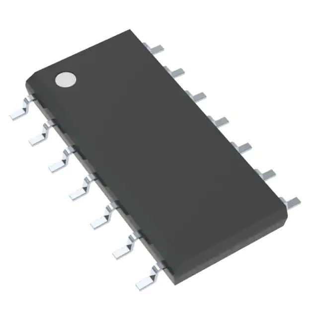
The CD4085BM96 types are supplied in 14-lead hermetic dual-in-line ceramic packages (F3A suffix), 14-lead dual-in-line plastic packages (E suffix), 14-lead small-outline packages (M, MT, M96, and NSR suffixes), and 14-lead thin shrink small-outline packages (PW and PWR suffixes).
Feature
- Medium-speed operation - tPHL = 90 ns; tPLH = 125 ns (typ.) at 10 V
- Individual inhibit controls
- Standardized symmetrical output characteristics
- 100% tested for quiescent current at 20 V
- Maximum input current of 1 μA at 18 V over full package-temperature range; 100 nA at 18 V and 25°C
- Noise margin (over full package-temperature range):
- 1 V at VDD = 5 V
- 2 V at VDD = 10 V
- 2.5 V at VDD = 15 V
- 5-V, 10-V, and 15-V parametric ratings
- Meets all requirements of JEDEC Tentative Standard No. 13B, "Standard Specifications for Description of 'B' Series CMOS Devices"


