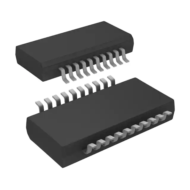
The CY74FCT2574ATQCT is a high-speed, low-power, octal D-type flip-flop featuring separate D-type inputs for each flip-flop. On-chip termination resistors at the outputs reduce system noise caused by reflections. The CY74FCT2574ATQCT can replace the CY74FCT574T to reduce noise in an existing design. This device has 3-state outputs for bus-oriented applications. A buffered clock (CP) and output-enable (OE\) inputs are common to all flip-flops. The CY74FCT2574ATQCT is identical to the CY74FCT2374T, except that on the CY74FCT2574ATQCT all outputs are on one side of the package and all inputs are on the other side. The flip-flops in the CY74FCT2574ATQCT store the state of their individual D inputs that meet the setup-time and hold-time requirements on the low-to-high CP transition. When OE\ is low, the contents of the flip-flops are available at the outputs. When OE\ is high, the outputs are in the high-impedance state. The state of OE\ does not affect the state of the flip-flops.
This device is fully specified for partial-power-down applications using Ioff. The Ioff circuitry disables the outputs, preventing damaging current backflow through the device when it is powered down.
Feature
- Function and Pinout Compatible With FCT and F Logic
- 25- Output Series Resistors to Reduce Transmission-Line Reflection Noise
- Reduced VOH (Typically = 3.3 V) Version of Equivalent FCT Functions
- Edge-Rate Control Circuitry for Significantly Improved Noise Characteristics
- Ioff Supports Partial-Power-Down Mode Operation
- Matched Rise and Fall Times
- Fully Compatible With TTL Input and Output Logic Levels
- ESD Protection Exceeds JESD 22
- 2000-V Human-Body Model (A114-A)
- 200-V Machine Model (A115-A)
- 1000-V Charged-Device Model (C101)
- 3-State Outputs
- 12-mA Output Sink Current 15-mA Output Source Current
- Edge-Triggered D-Type Inputs
- 250-MHz Typical Switching Rate
The CY74FCT2574T is a high-speed, low-power, octal D-type flip-flop featuring separate D-type inputs for each flip-flop. On-chip termination resistors at the outputs reduce system noise caused by reflections. The CY74FCT2574T can replace the CY74FCT574T to reduce noise in an existing design. This device has 3-state outputs for bus-oriented applications. A buffered clock (CP) and output-enable (OE\) inputs are common to all flip-flops. The CY74FCT2574T is identical to the CY74FCT2374T, except that on the CY74FCT2574T all outputs are on one side of the package and all inputs are on the other side. The flip-flops in the CY74FCT2574T store the state of their individual D inputs that meet the setup-time and hold-time requirements on the low-to-high CP transition. When OE\ is low, the contents of the flip-flops are available at the outputs. When OE\ is high, the outputs are in the high-impedance state. The state of OE\ does not affect the state of the flip-flops.
This device is fully specified for partial-power-down applications using Ioff. The Ioff circuitry disables the outputs, preventing damaging current backflow through the device when it is powered down.


