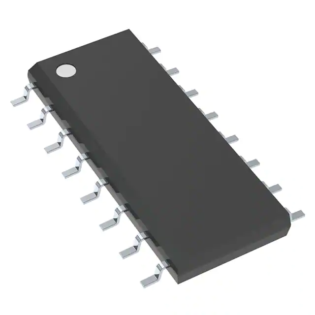
This positive-edge-triggered D-type flip-flop has a direct clear (CLR)\ input. The CD74AC175M96E4 features complementary outputs from each flip-flop.
Information at the data (D) inputs meeting the setup time requirements is transferred to the outputs on the positive-going edge of the clock (CLK) pulse. Clock triggering occurs at a particular voltage level and is not directly related to the transition time of the positive-going edge of CLK. When CLK is at either the high or low level, the D input has no effect at the output.
Feature
- AC Types Feature 1.5-V to 5.5-V Operation and Balanced Noise Immunity at 30% of the Supply Voltage
- Buffered Inputs
- Contains Four Flip-Flops With Double-Rail Outputs
- Speed of Bipolar F, AS, and S, With Significantly Reduced Power Consumption
- Balanced Propagation Delays
- ±24-mA Output Drive Current
- Fanout to 15 F Devices
- SCR-Latchup-Resistant CMOS Process and Circuit Design
- Exceeds 2-kV ESD Protection Per MIL-STD-883, Method 3015
- Applications Include:
- Buffer/Storage Registers
- Shift Registers
- Pattern Generators
This positive-edge-triggered D-type flip-flop has a direct clear (CLR)\ input. The CD74AC175 features complementary outputs from each flip-flop.
Information at the data (D) inputs meeting the setup time requirements is transferred to the outputs on the positive-going edge of the clock (CLK) pulse. Clock triggering occurs at a particular voltage level and is not directly related to the transition time of the positive-going edge of CLK. When CLK is at either the high or low level, the D input has no effect at the output.


