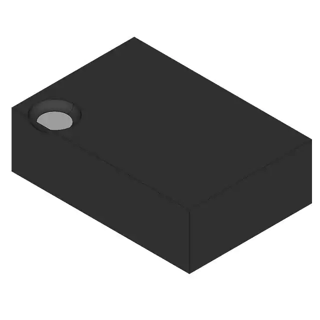
The 74AXP1G58 is a configurable multiple function gate with Schmitt-trigger inputs. The device can be configured as any of the following logic functions AND, OR, NAND, NOR, XOR, inverter and buffer. All inputs can be connected directly to VCC or GND. This device ensures very low static and dynamic power consumption across the entire VCC range from 0.7 V to 2.75 V. This device is fully specified for partial power down applications using IOFF. The IOFF circuitry disables the output, preventing the potentially damaging backflow current through the device when it is powered down.
The is a configurable multiple function gate with Schmitt-trigger inputs. The device can be configured as any of the following logic functions AND, OR, NAND, NOR, XOR, inverter and buffer. All inputs can be connected directly to VCC or GND. This device ensures very low static and dynamic power consumption across the entire VCC range from 2.75 V. This device is fully specified for partial power down applications using IOFF. The IOFF circuitry disables the output, preventing the potentially damaging backflow current through the device when it is powered down.
Wide supply voltage range from 2.75 V High noise immunity Complies with JEDEC standard: JESD8-12A.01 (wide range: V) JESD8-12A.01 (normal range: 2.7 V) ESD protection: HBM ANSI/ESDA/JEDEC JS-001 Class 2 exceeds 2 kV CDM JESD22-C101E exceeds 1000 V Low static power consumption; ICC (85 C maximum) Latch-up performance exceeds 100 mA per JESD 78 Class II Inputs accept voltages 2.75 V Low noise overshoot and undershoot % of VCC IOFF circuitry provides partial power-down mode operation Multiple package options Specified from +85 C
Table 1. Ordering information Package Temperature range +85 C Name XSON6 Description Version plastic extremely thin small outline package; no leads; SOT886 6 terminals; body 0.5 mm extremely thin small outline package; no leads; 6 terminals; body 0.35 mm extremely thin small outline package; no leads; 6 terminals; body SOT1115 SOT1202 Type number
The pin 1 indicator is located on the lower left corner of the device, below the marking code.All information provided in this document is subject to legal disclaimers.
Table 3. Symbol B GND A Y VCC C Pin description Pin Description data input ground (0 V) data input data output supply voltage data input


