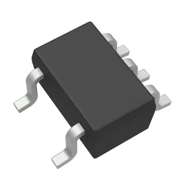
The SN74AUP1T32DCKR performs the Boolean function Y = A + B or Y = VT = 210 mV between positive and negative input transitions) offer improved noise immunity during switching transitions, which is especially useful on analog mixed-mode designs. Schmitt-trigger inputs reject input noise, ensure integrity of output signals, and allow for slow input signal transition.
Ioff is a feature that allows for powered-down conditions (VCC = 0 V) and is important in portable and mobile applications. When VCC = 0 V, signals in the range from 0 V to 3.6 V can be applied to the inputs and outputs of the device. No damage occurs to the device under these conditions.
The SN74AUP1T32DCKR is designed with optimized current-drive capability of 4 mA to reduce line reflections, overshoot, and undershoot caused by high-drive outputs.
Feature
- Single-Supply Voltage Translator
- Output Level Up to Supply VCC CMOS Level
- 1.8 V to 3.3 V (at VCC = 3.3 V)
- 2.5 V to 3.3 V (at VCC = 3.3 V)
- 1.8 V to 2.5 V (at VCC = 2.5 V)
- 3.3 V to 2.5 V (at VCC = 2.5 V
- Schmitt-Trigger Inputs Reject Input Noise and Provide Better Output Signal Integrity
- Ioff Supports Partial Power Down (VCC = 0 V)
- Very Low Static Power Consumption: 0.1 μA
- Very Low Dynamic Power Consumption: 0.9 μA
- Latch-Up Performance Exceeds 100 mA Per JESD 78, Class II
- Pb-Free Packages Available: SC-70 (DCK) 2 × 2.1 × 0.65 mm (Height 1.1 mm)
- More Gate Options Available at www.ti.com/littlelogic
- ESD Performance Tested Per JESD 22
- 2000-V Human-Body Model (A114-B, Class II)
- 1000-V Charged-Device Model (C101)
The SN74AUP1T32 performs the Boolean function Y = A + B or Y = VT = 210 mV between positive and negative input transitions) offer improved noise immunity during switching transitions, which is especially useful on analog mixed-mode designs. Schmitt-trigger inputs reject input noise, ensure integrity of output signals, and allow for slow input signal transition.
Ioff is a feature that allows for powered-down conditions (VCC = 0 V) and is important in portable and mobile applications. When VCC = 0 V, signals in the range from 0 V to 3.6 V can be applied to the inputs and outputs of the device. No damage occurs to the device under these conditions.
The SN74AUP1T32 is designed with optimized current-drive capability of 4 mA to reduce line reflections, overshoot, and undershoot caused by high-drive outputs.


