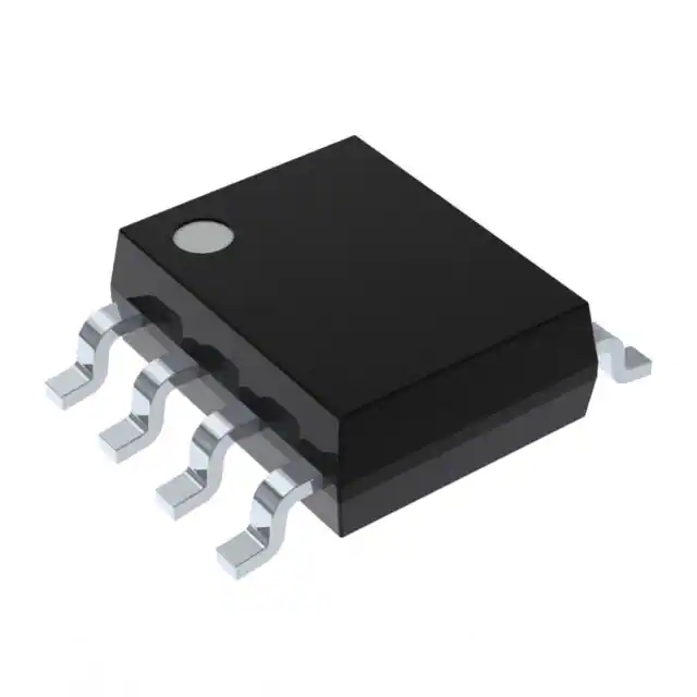
The MAX1822ESA high-side supply, using a regulated charge pump, generates a regulated output voltage 11V greater than the input supply voltage to power high-side switching and control circuits. The MAX1822ESA allows low-resistance N-channel MOSFETs (FETs) to be used in circuits that normally require costly, less efficient P-channel FETs and PNP transistors. The high-side output also eliminates the need for logic FETs in +5V and other low-voltage switching circuits. A +3.5V to +16.5V input supply range and a typical quiescent current of only 150μA make the MAX1822ESA ideal for a wide range of line- and battery-powered switching and control applications where efficiency is crucial. Also provided is a logic-level power-ready output (PR) to indicate when the high-side voltage reaches the proper level. The MAX1822ESA comes in an 8-pin SO package and requires three inexpensive external capacitors. The MAX1822ESA is a pin-for-pin replacement to the MAX622.
Feature
- +3.5V to +16.5V Operating Supply Voltage Range
- Output Voltage Regulated to VCC + 11V (typ)
- 150μA (typ) Quiescent Current
- Power-Ready Output
Applications
- Battery Management
- H-Switches
- High-Side Power Control with N-Channel FETs
- Low-Dropout Voltage Regulators
- Portable Computing
- Power Switching from Low Supply Voltages
- Stepper Motor Drivers


