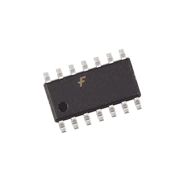
The LCX14 contains six inverter gates each with a Schmitt trigger input. They are capable of transforming slowly changing input signals into sharply defined, jitter-free output signals. In addition, they have a greater noise margin than conventional inverters. The LCX14 has hysteresis between the positive-going and negative-going input thresholds (typically 1.0V) which is determined internally by transistor ratios and is essentially insensitive to temperature and supply voltage variations. The inputs tolerate voltages up to 7V allowing the interface of 5V, 3V and 2.5V systems. The 74LCX14SJX is fabricated with advanced CMOS technology to achieve high speed operation while maintaining CMOS low power dissipation.
Feature
- 5V tolerant inputs
- 2.3V-3.6V VCC specifications provided
- 6.5 ns tPD max (VCC = 3.3V), 10 µA ICC max
- Power down high impedance inputs and outputs
- ±24 mA output drive (VCC = 3.0V)
- Implements patented noise/EMI reduction circuitry
- Latch-up performance exceeds JEDEC 78 conditions
- ESD performance: Machine model > 200V Human model > 2000V
- Leadless Pb-Free DQFN package
Applications
- This product is general usage and suitable for many different applications.


