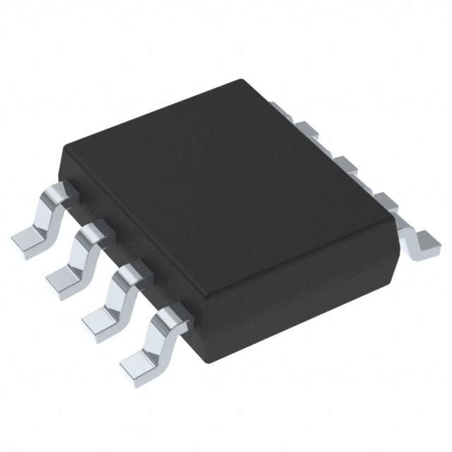
The TPS5432DDA is a 6V, 3A, low Iq, current mode, synchronous monolithic buck converter with integrated MOSFETs. The TPS5432DDA enables small designs by integrating the MOSFETs, implementing current mode control to reduce external component count, reducing inductor size by 700kHz switching frequency. SOIC-8 package with exposed thermal pad provides both thermally enhanced solution and easy to use.
The TPS5432DDA provides accurate regulation for a variety of loads with an accurate 3.0% voltage reference over temperature.
Efficiency is maximized through the integrated 70m? MOSFETs and 360μA typical supply current. Using the enable pin, shutdown supply current is reduced to 2 μA by entering a shutdown mode.
The output voltage startup ramp is controlled by the slow start pin. A ceramic capacitor at this pin can easily adjust the slow start time.
Frequency fold back and thermal shutdown protects the device during an over-current condition.
Feature
- Two 70mΩ (typical) MOSFETs for 3A Continuous Output Current
- Current Mode Control With External Compensation
- 700kHz Switching Frequency
- 360μA no Load Quiescent Operating Current (no switching)
- 0.808V Internal Voltage Reference
- ±2.0% Reference Accuracy at 25°C
- ±3.0% Reference Accuracy Over Temperature Range –40°C~125°C
- Stable Operation With Ceramic Output Capacitor
- Adjustable Slow Start
- Cycle by Cycle Current Limit, and Frequency Fold Back Protection
- Thermally Enhanced 8-Pin SOIC (DDA) Package
The TPS5432 is a 6V, 3A, low Iq, current mode, synchronous monolithic buck converter with integrated MOSFETs. The TPS5432 enables small designs by integrating the MOSFETs, implementing current mode control to reduce external component count, reducing inductor size by 700kHz switching frequency. SOIC-8 package with exposed thermal pad provides both thermally enhanced solution and easy to use.
The TPS5432 provides accurate regulation for a variety of loads with an accurate 3.0% voltage reference over temperature.
Efficiency is maximized through the integrated 70m? MOSFETs and 360μA typical supply current. Using the enable pin, shutdown supply current is reduced to 2 μA by entering a shutdown mode.
The output voltage startup ramp is controlled by the slow start pin. A ceramic capacitor at this pin can easily adjust the slow start time.
Frequency fold back and thermal shutdown protects the device during an over-current condition.


